
Power amplifier

a power amplifier and amplifier technology, applied in the field of radio frequency (rf) transmission, can solve the problems of limiting bandwidth, reducing the efficiency of the overall system, and compromising the overall system efficiency, and achieve the effect of reducing the complexity of the circuitry and high output impedan

Active Publication Date: 2011-10-06
SONY EUROPE BV
View PDF2 Cites 24 Cited by
  • Summary
  • Abstract
  • Description
  • Claims
  • Application Information

AI Technical Summary

Benefits of technology

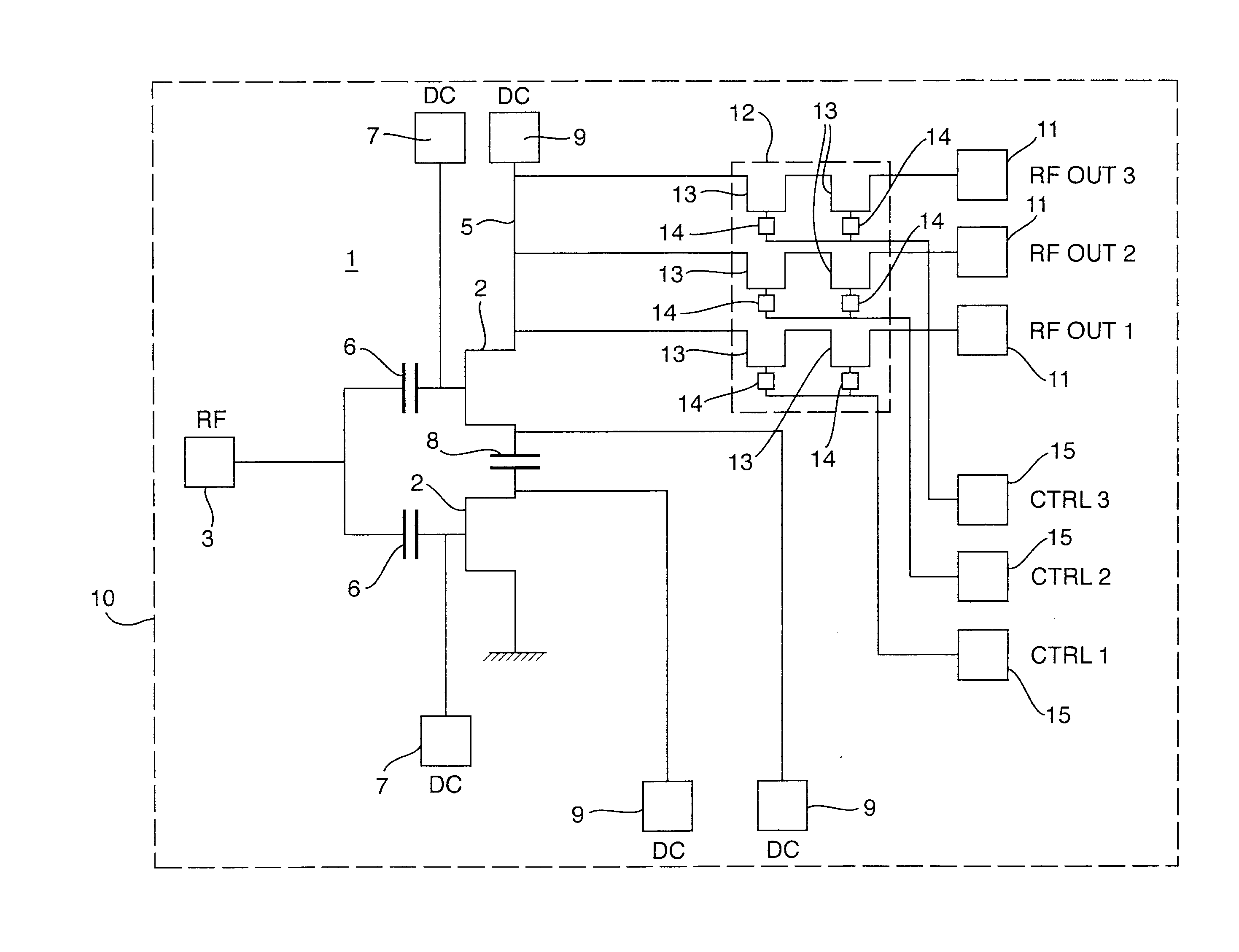
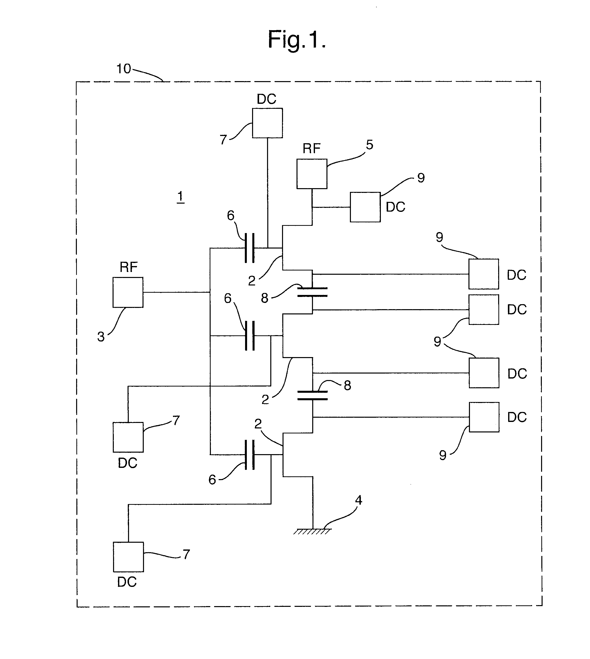
The present invention provides a power amplifier for amplifying an RF input signal. The power amplifier includes an amplifier input for receiving the RF input signal and an amplifier output for outputting an amplified RF output signal. The power amplifier also includes a series stack of power amplifier devices, each arranged to amplify a signal supplied to an input terminal thereof and to generate an amplified signal across two output terminals thereof. The output terminals of each power amplifier device are connected in series to the amplifier output. The power amplifier also includes a respective intermediate coupling capacitor connected between the output terminals of each adjacent pair of power amplifier devices for DC isolation of the power amplifier devices. The technical effect of the present invention is that the power amplifier provides improved efficiency and flexibility in accommodating variation in the output voltage of the power supply, while also allowing individual power amplifier devices to be shorted out to improve overall efficiency and improve the effective battery life.

Problems solved by technology

Such a combination of a small supply voltage and a high capacitance leads to the power amplifiers being of low impedance and high Q-factor, thus limiting the bandwidth.
Another issue with power amplifiers is efficiency, because power amplifiers contribute a significant proportion of the power consumption of a mobile telecommunications device.
Such schemes require linear power amplification that compromises overall system efficiency, for example requiring power amplifiers to be backed off from saturated maximum power.
The voltage applied across an individual semiconductor device is limited by the physical material properties of the semiconductor as high voltages can cause breakdown.
Another issue in portable telecommunication devices is the discharge characteristic of batteries typically used as a power supply.
When the actual output voltage of the battery is above the nominal output voltage, then the efficiency of the components is compromised, because the power derived from the actual DC bias voltage in excess of the nominal output voltage is effectively wasted.
This impacts on the power consumption.

Method used


Image

  • Power amplifier
  • Power amplifier
  • Power amplifier

Examples


Embodiment Construction

[0045]The power amplifier 1 comprises a series stack of transistors 2 that constitute power amplifier devices. In the examples shown in FIG. 1, the power amplifier 1 includes three transistors 2. However, this is merely by way of example and in general the power amplifier 1 may include any plural number of transistors 2. In this example, the transistors 2 are junction pseudomorphic high electron-mobility transistors (JPHEMTs). This technology exhibits several attractive characteristics compared to alternative power amplifier devices, such as having a high Gm at turn-on and a linear Gm / bias characteristic.

[0046]The power amplifier 1 also has an amplifier input 3 for receiving a radio frequency (RF) input signal. The gates of the individual transistors 2, that act as input terminals thereof, are connected in parallel to the amplifier input 3 so that the transistors 2 each receive the RF input signal. In operation, each transistor 2 amplifies the RF input signal supplied thereto, and g...


PUM


Abstract

A power amplifier comprises a series stack of power amplifier devices, connected in parallel to the amplifier input for receiving an RF input signal, and having output terminals being connected in series to the amplifier output. An intermediate coupling capacitor is connected between each adjacent pair of power amplifier devices in the series stack of power amplifier devices for DC isolation of said power amplifier devices. This reduces the required DC supply voltage, as well as allowing shorting of individual power amplifier devices in response to variation in the DC supply voltage.

Description

CROSS-REFERENCE TO RELATED APPLICATIONS[0001]This application is based upon and claims the benefit of priority from British Application No. 10054963 filed 31 Mar. 2010, the entire contents of which are incorporated by reference.BACKGROUND OF THE INVENTION[0002](1) Field of the Invention[0003]The present invention relates to radio frequency (RF) transmission in portable telecommunication devices and specifically to power amplifiers for amplifying RF signals for transmission.[0004](2) Description of Related Art[0005]As portable telecommunication devices are developed, the number of frequency bands in usage is increasing rapidly. Many 3G standards have been developed, characterised by ever-increasing numbers of frequency bands. The number of frequency bands is further increasing as 4G standards are developed and implemented.[0006]Components for portable telecommunication devices are typically designed to be capable of operation in multiple different frequency bands. This is to allow op...

Claims


Application Information

Patent Timeline
Patent Type & Authority Applications(United States)
IPC IPC(8): H03F3/68
CPCH03F1/0222H03F2203/7236H03F1/0277H03F3/193H03F3/211H03F3/245H03F3/72H03F2200/111H03F2200/171H03F2200/18H03F2200/27H03F2200/271H03F2200/366H03F2200/405H03F2200/414H03F2200/417H03F2200/421H03F2200/429H03F2200/451H03F2200/471H03F2200/504H03F2200/507H03F2200/511H03F2200/516H03F2200/525H03F2200/54H03F2203/21145H03F2203/21157H03F2203/21175H03F2203/21178H03F2203/21193H03F2203/7206H03F2203/7209H03F2203/7227H03F1/0261H03F3/604
Inventor CLIFTON, JOHN CHRISTOPHER
Owner SONY EUROPE BV
Learn More