Spin memory and spin transistor
a spin memory and transistor technology, applied in semiconductor devices, digital storage, instruments, etc., can solve the problems of increasing the total circuit area, unable to use the so-called cross-point architecture, and unable to make the cell size equal or smaller than the cell size of a dynamic random access memory (dram)
- Summary
- Abstract
- Description
- Claims
- Application Information
AI Technical Summary
Problems solved by technology
Method used
Image
Examples
first embodiment
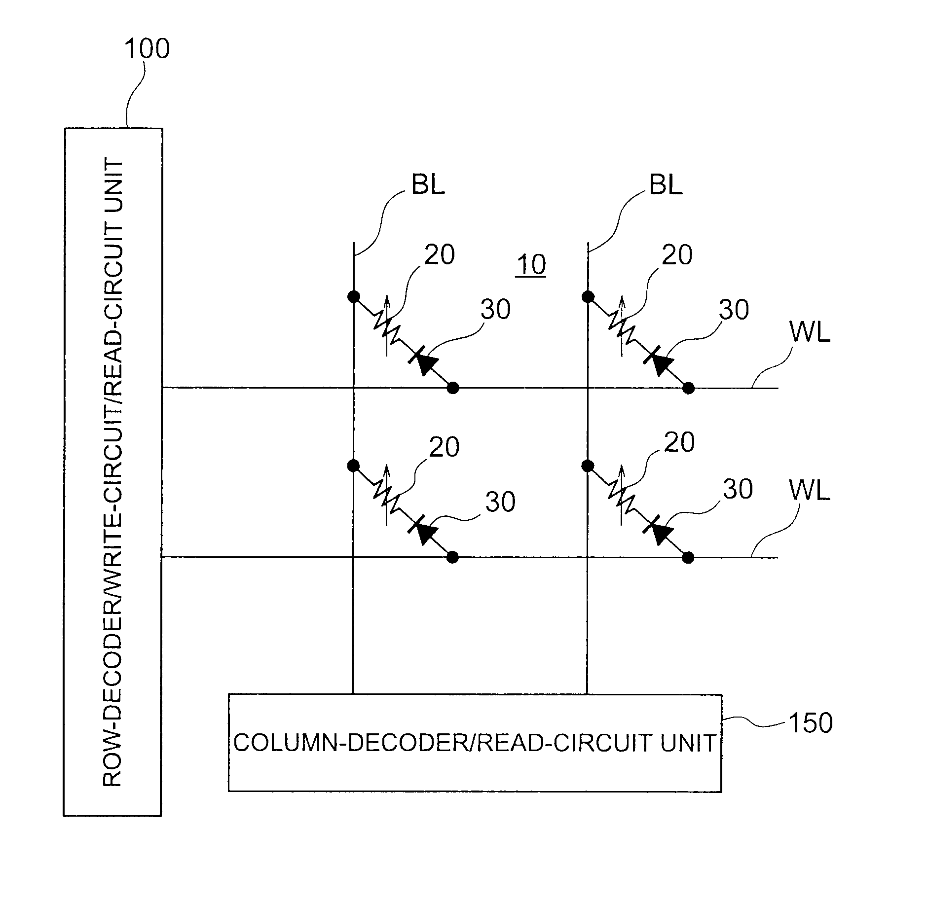
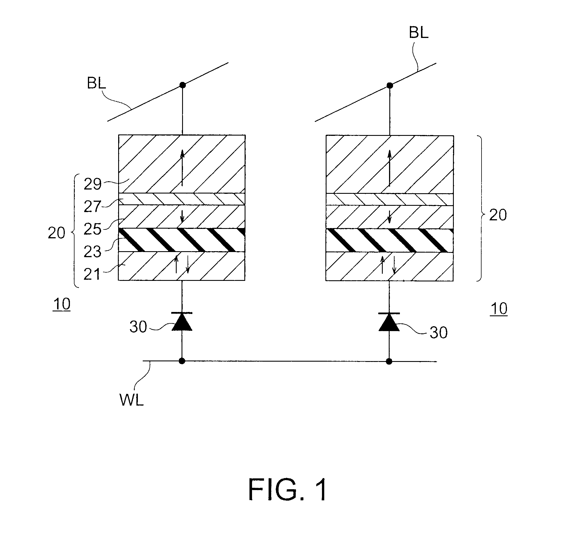
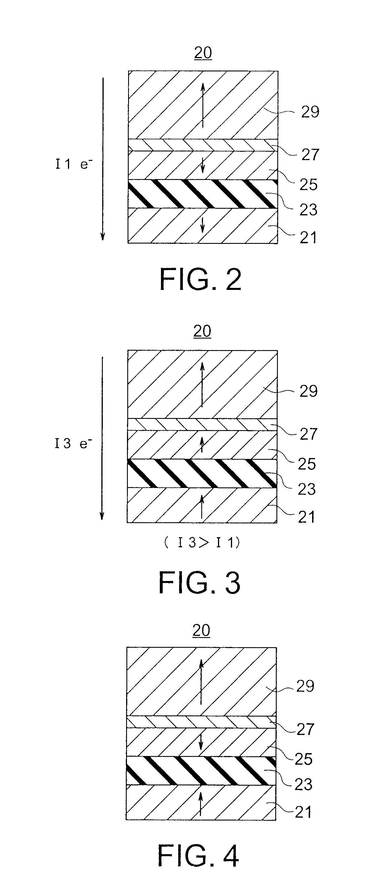
[0025]FIG. 1 shows a spin memory according to a first embodiment of the present invention. The spin memory of the first embodiment has memory cells 10 (two memory cells 10 in FIG. 1) arranged in a matrix fashion. Each of the memory cells 10 includes a ferromagnetic stacked film 20 and a diode 30. The ferromagnetic stacked film 20 has a stacked structure in which a ferromagnetic layer 21, a nonmagnetic layer 23, a ferromagnetic layer 25, a nonmagnetic layer 27, and a ferromagnetic layer 29 are stacked in this order. The ferromagnetic layer 21, the ferromagnetic layer 25, and the ferromagnetic layer 29 each have an easy axis of magnetization that is substantially perpendicular to the film plane. Specifically, when there is not an external magnetic field, the magnetization direction of each of the ferromagnetic layers is substantially perpendicular to the film plane. Here, the film plane means the upper face of each ferromagnetic layer. The magnetization reversal magnetic fields of the...
second embodiment
[0047]FIG. 7 shows a spin transistor according to a second embodiment of the present invention. The spin transistor of the second embodiment is a spin transistor that is formed on a semiconductor layer 41. Here, a “semiconductor layer” means a semiconductor substrate, a well region formed in a semiconductor substrate, a SOI (Silicon On Insulator) layer in a SOI substrate, or the like. An impurity region 43a and an impurity region 43b that are doped with impurities at high density are provided at a distance from each other on the surface of the semiconductor layer 41. In this embodiment, the semiconductor layer 41 is an n-type semiconductor layer, the impurity region 43a and the impurity region 43b are a p-type impurity region 43a and a p-type impurity region 43b, and the spin transistor is a p-type spin transistor. In this case, the p-type impurity region 43a and the p-type impurity region 43b are to be a source region 43a and a drain region 43b. A channel region 42 is formed in a p...
third embodiment
[0060]Next, a spin transistor according to a third embodiment of the present invention is described. The spin transistor of the second embodiment illustrated in FIG. 7 is of a transverse type, and has a structure in which the source electrode and the source region having ferromagnetic layers are placed on a side of the channel region, and the drain region and the drain electrode are placed on the other side of the channel region. The spin transistor of the third embodiment is of a longitudinal type, and has a structure in which a source electrode, a channel region, and a drain electrode are stacked in this order on a semiconductor layer.
[0061]FIG. 13 shows the spin transistor of the third embodiment. The spin transistor of this third embodiment is placed on a SOI substrate 70 that includes a supporting substrate 71 made of Si, a buried oxide film 72, and a SOI layer 73. The spin transistor of the third embodiment may be placed on a bulk substrate made of Si, instead of a SOI substra...
PUM
 Abstract
Description
Claims
Application Information
 - R&D
- Intellectual Property
- Life Sciences
- Materials
- Tech Scout
- Unparalleled Data Quality
- Higher Quality Content
- 60% Fewer Hallucinations
Browse by: Latest US Patents, China's latest patents, Technical Efficacy Thesaurus, Application Domain, Technology Topic, Popular Technical Reports.
© 2025 PatSnap. All rights reserved.Legal|Privacy policy|Modern Slavery Act Transparency Statement|Sitemap|About US| Contact US: help@patsnap.com


