Plasma display panel and chamber for manufacturing plasma display panel

a technology of plasma display panel and plasma display panel, which is applied in the direction of electrical apparatus casing/cabinet/drawer, gas exhaustion means, etc., can solve the problems of difficult to use the technique in a pdp, constrained thickness of pdp, and difficulty in pdp thickness, etc., to achieve low melting point, improve the degree of freedom of panel design, and reduce the effect of cos

Active Publication Date: 2011-09-15
PANASONIC CORP
View PDF6 Cites 2 Cited by
  • Summary
  • Abstract
  • Description
  • Claims
  • Application Information

AI Technical Summary

Benefits of technology

A plasma display panel according to a typical embodiment of the present invention comprises a front glass substrate and a rear glass substrate, the plasma display panel sealing a discharge gas in between the front glass substrate and the rear glass substrate, wherein a hole for filling of the discharge gas is provided in the front glass substrate or the rear glass substrate, and a plug sealant is attached between the front glass substrate and the rear glass substrate in a sealing manner so as to prevent entry of the atmosphere from the hole.
The plasma display panel can be configured such that the bank is for preventing leakage of the sealant in a display region of the plasma display panel.
According to the PDP of the present invention, a gas filling pipe or an exhausting pipe becomes unnecessary and thus a thickness of the panel can be set at a thickness of the front glass substrate, the rear glass substrate, and a low melting point glass seal for sealing them.
Further, since an exhausting pipe which is not related to the structure of the PDP and a step / equipment for mounting the exhausting pipe become unnecessary, a cost reduction can be expected. Furthermore, it is not necessarily required to provide a hole for exhausting / filling gas on the rear glass substrate, and thus a degree of freedom for panel design is improved.

Problems solved by technology

Meanwhile, each of the techniques described in the above-mentioned Patent Documents has problems.
In the technique described in Japanese Patent Application Laid-Open Publication No. 2005-303065, since an opening is provided on a side of the package, it is difficult to use the technique in a PDP having a structure in which the front glass substrate and the rear glass substrate are attached to each other.
Therefore, there is a problem that the thickness of the PDP is constrained according to the length of the exhaust pipe.
H11-240739, since joining using a fritted glass or the like is performed upon attaching an exhaust pipe which has no relationship with manufacture of the PDP, there is such a problem that the number of manufacturing steps increases.

Method used


Image

  • Plasma display panel and chamber for manufacturing plasma display panel
  • Plasma display panel and chamber for manufacturing plasma display panel
  • Plasma display panel and chamber for manufacturing plasma display panel

Examples


first embodiment

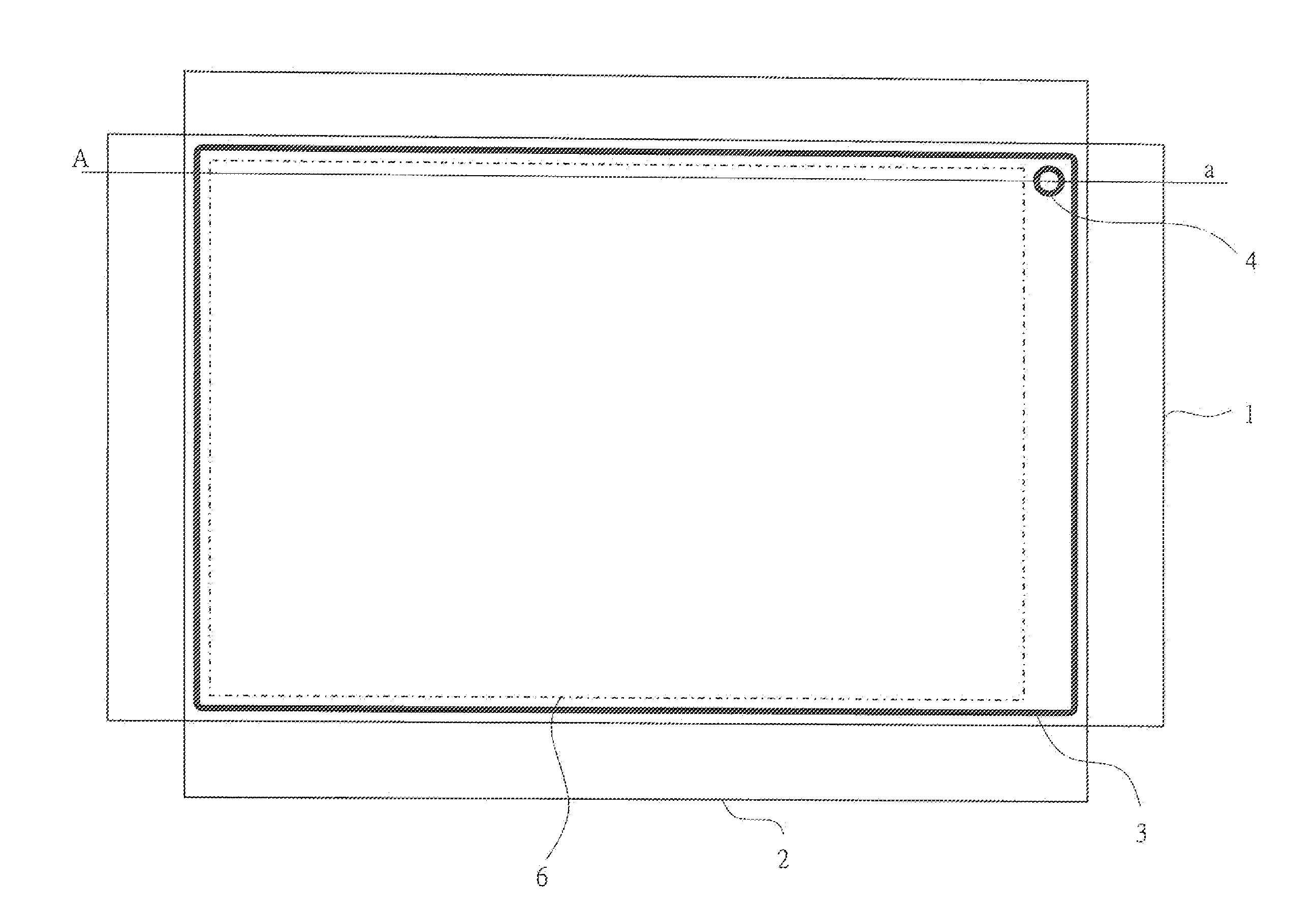
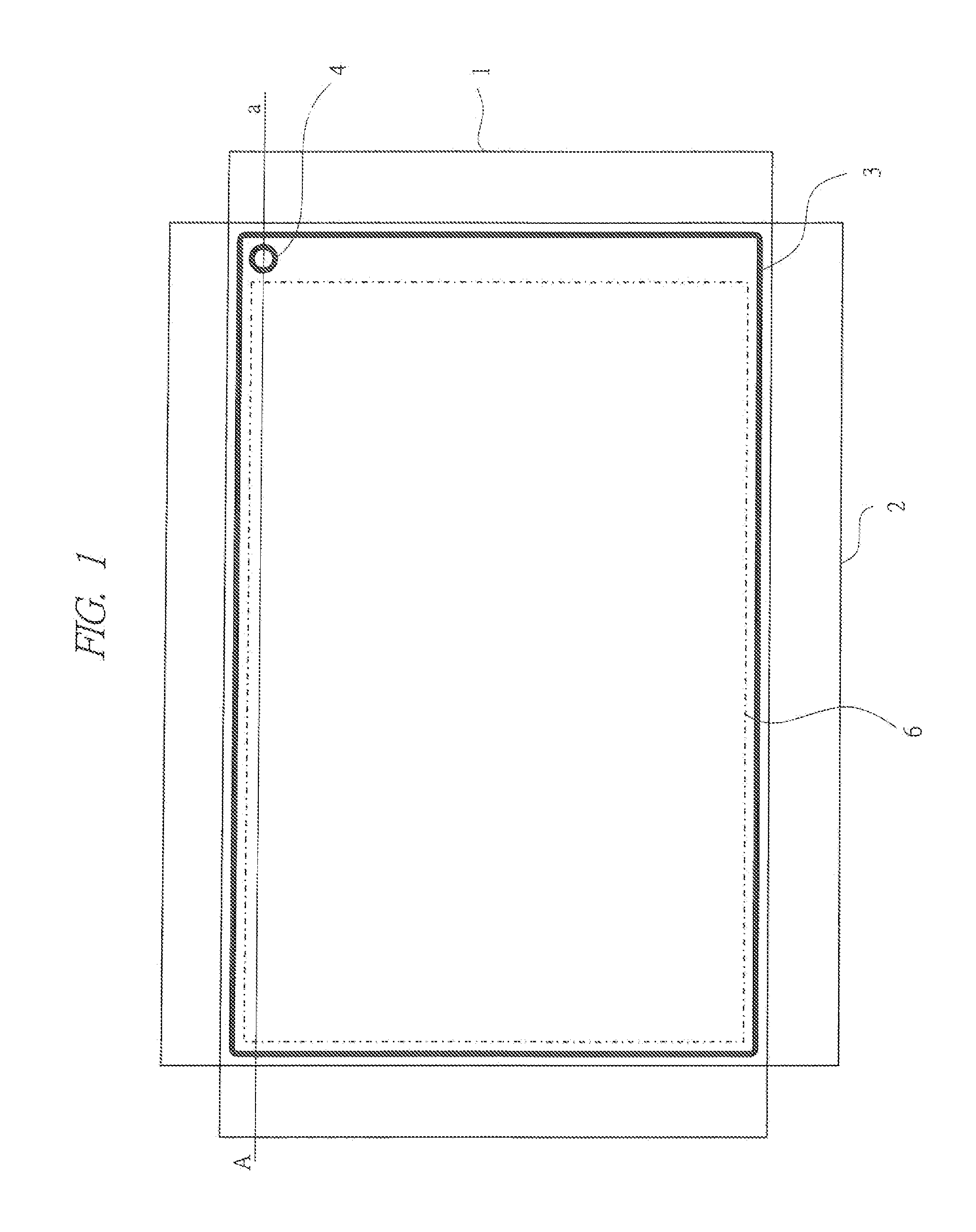
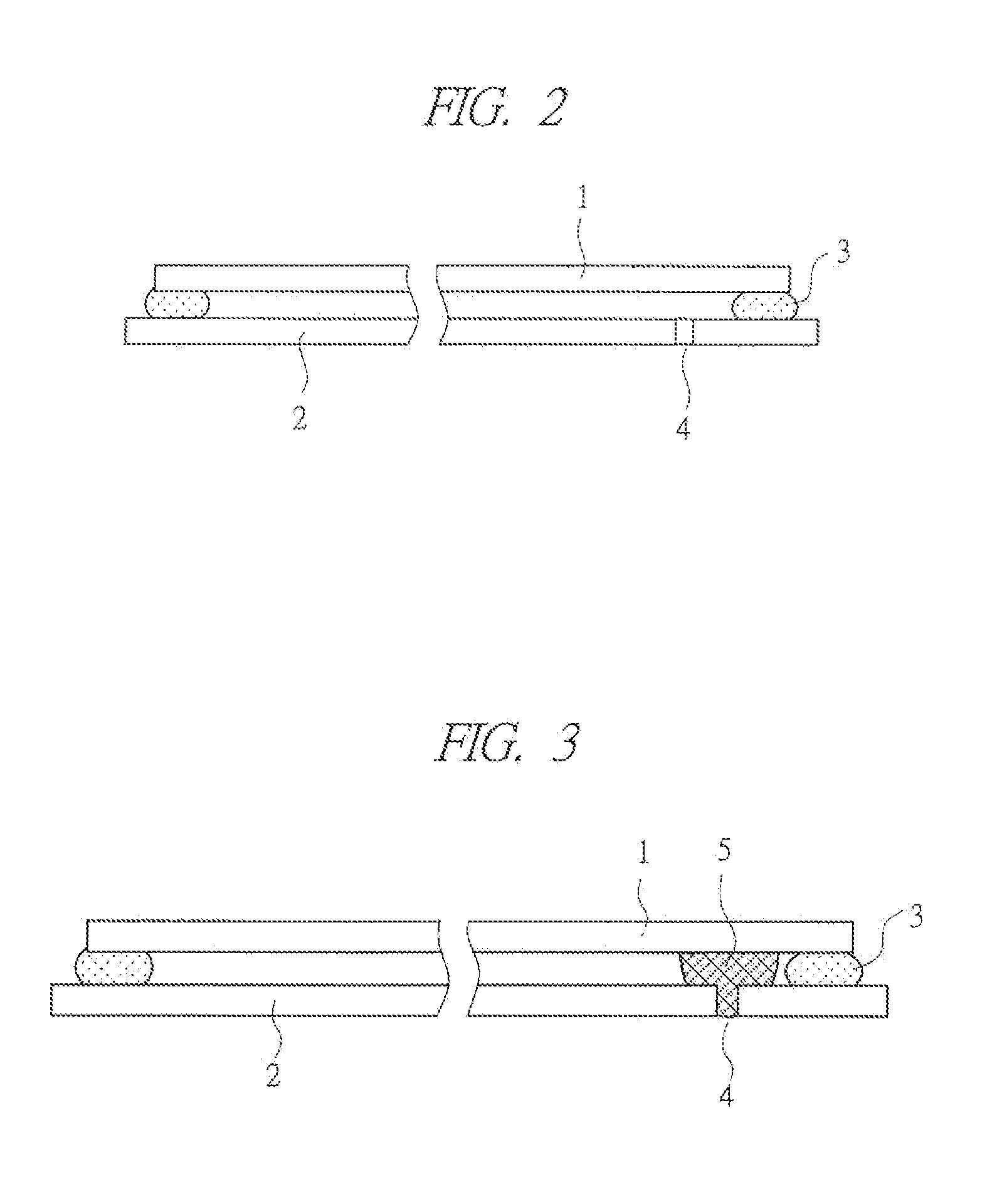
FIG. 1 is a top perspective view of an AC-type PDP using a structure according to a first embodiment of the present invention. Further, FIG. 2 is a cross-sectional view of the AC-type PDP using the structure according to the first embodiment of the present invention before it is sealed. The cross-sectional view illustrated in FIG. 2 is a cross-sectional view of the AC-type PDP taken along the line A-a in FIG. 1. FIG. 3 is cross-sectional view of the AC-type PDP using the structure according to the first embodiment of the present invention after it is sealed.

The AC-type PDP is configured to include a front glass substrate 1, a rear glass substrate 2, a seal 3, a gas-filling hole 4, and a plug sealant 5 (shown in FIG. 3).

The front glass substrate 1 is a glass substrate constituting a display screen of a plasma display television set serving as a display device. The front glass substrate 1 is composed of display electrode pairs made of an ITO and metal electrodes, a dielectric layer, a...

second embodiment

Next, a second embodiment of the present invention will be described with reference to the attached drawings.

In the first embodiment, there has not been any restraint on post-supply of the solder supplied to the gas filling hole 4. Therefore, when adjustment of the supplied amount of the solder is unsuccessful, there is a possibility that the solder flows into structural bodies related to the display area 6 (the ribs on the rear glass substrate 2 or the like).

In the second embodiment, a configuration to prevent such a problem from occurring will be proposed.

FIG. 7 is a top perspective view of an AC-type PDP using a structure according to the second embodiment of the present invention. Further, FIG. 8A is a cross-sectional view of the AC-type PDP using the structure related to the present invention before it is sealed. FIG. 8B is a cross-sectional view of the AC-type PDP using the structure related to the present invention after it has been sealed.

As viewed in FIG. 7, a bank 7 having...


PUM

PropertyMeasurementUnit
Temperatureaaaaaaaaaa
Thicknessaaaaaaaaaa
Diameteraaaaaaaaaa

Abstract

A structure of a panel which can be thinned down to about a panel thickness of a PDP and a manufacturing method thereof are provided. A gas filling hole is provided to a surface of a rear glass substrate of a PDP, the surface coming in contact with a front glass substrate of the PDP. Vacuuming and filling of a discharge gas are performed through the gas filling hole. After filling of the discharge gas, a mechanism for lifting solder iron up and down and supplying solder provided inside a chamber inserts a tip of an ultrasonic soldering iron into the gas filling hole to start supplying a solder which is a material for a plug sealant. When a series of forming steps of the plug sealant are finished, the ultrasonic soldering iron is retreated before the solder is solidified to finish formation of the plug sealant.

Description

CROSS-REFERENCE TO RELATED APPLICATIONThe present application claims priority from Japanese Patent Application No. 2010-051972 filed on Mar. 9, 2010, the content of which is hereby incorporated by reference into this application.TECHNICAL FIELD OF THE INVENTIONThe present invention relates to a structure of a plasma display panel used as a display device, and a chamber for manufacturing the same.BACKGROUND OF THE INVENTIONPlasma display panels (PDPs) are products which draw attention as full-color display devices suitable for large screens and which have spread widely. In an AC-type PDP of a three-electrode surface-discharge type, a plurality of sustain electrode pairs for generating surface discharge on a glass substrate on a display side (front glass substrate) are formed of ITO or the like. Address electrodes formed to be perpendicular to the sustain electrode pairs as viewed from a display area and a phosphor layer covering the address electrodes are formed on a glass substrate ...

Claims


Application Information

Patent Timeline
IPC IPC(8): H01J5/00H01J9/38H01J9/385H01J9/395H01J11/12H01J11/24H01J11/26H01J11/36H01J11/46H01J11/48H01J11/54
CPCH01J9/40H01J11/48H01J11/10H01J17/49H01J17/18
Inventor KASAHARA, SHIGEOTOKAI, AKIRAINOUE, MANABUKOSUGI, NAOKIYOSHITANI, TOSHIAKI
Owner PANASONIC CORP
Why Eureka
Try Eureka