Methods and Compositions for Preparing Tensile Strained Ge on Ge1-ySNy Buffered Semiconductor Substrates

a technology of strained ge and buffered semiconductors, applied in the direction of basic electric elements, electrical equipment, semiconductor devices, etc., can solve the problems of non-uniform and potentially defective interfaces, stress as a perturbation, and lack of precise strain control, so as to achieve high reactivity

Inactive Publication Date: 2011-08-18
ARIZONA STATE UNIVERSITY
View PDF12 Cites 3 Cited by
  • Summary
  • Abstract
  • Description
  • Claims
  • Application Information

AI Technical Summary

Benefits of technology

[0013]Herein is provided an approach based for the generation of tensile-strained Ge epilayers based on the creation of Ge1-ySny alloys with tunable lattice dimensions above that of Ge which serve as the critical facilitating platforms for the subsequent tensile-Ge growth. In addition this approach subsumes the following distinctive features: (i) low growth temperature that promotes the assembly of highly-strained tetragonally-distorted Ge structures that remain robust despite the inherent metastability. (ii) layer-by-layer growth mechanisms leading to flat surfaces, chemically abrupt interfaces devoid of chemical intermixing and relatively defect free layer microstructures. Both features are enabled by exploiting the high reactivity and the pseudo-surfactant behavior of the (GeH3)2CH2 species. Collectively this methodology has allowed the systematic production of Ge layers with very high tensile strains and all of the desired morphological and structural properties as discussed below. Thereby, the utility of Ge can be extended into the wider infrared optoelectronic domain by tuning its fundamental optical properties using strain as a main parameter

Problems solved by technology

The use of stress as a perturbation is problematic because the direct band gap can only be lowered with tensile strain.
Further limitations of the thermal expansion process include lack of precise strain control and a maximum predicted strain value of 0.3% for growth at 900° C.
Moreover, the use of high temperatures (800-900° C.) typically induces inter-diffusion of the elements across the Si—Ge heterojunction, resulting in non-uniform and potentially defective interfaces.
In the context of laser applications, spatial confinement requires abrupt interfaces, which are precluded using this high temperature process due to the inherent elemental intermixing at the interface.
In addition, precise and systematic control of the final strain state has not been demonstrated using this method, and this hampers the design of devices.

Method used


Image

  • Methods and Compositions for Preparing Tensile Strained Ge on Ge1-ySNy Buffered Semiconductor Substrates
  • Methods and Compositions for Preparing Tensile Strained Ge on Ge1-ySNy Buffered Semiconductor Substrates
  • Methods and Compositions for Preparing Tensile Strained Ge on Ge1-ySNy Buffered Semiconductor Substrates

Examples


example 1

General Deposition Procedures

Example 1a

GeSn Buffer Deposition

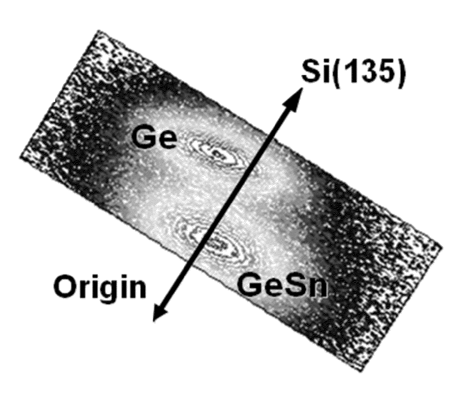
[0047]Ge1-ySny buffer layers (y=0.02-0.04) were deposited on hydrogen-passivated Si(100) wafers at 330-350° C., as described previously (see, Bauer et al., Appl. Phys. Lett. 81, 2992 (2002), which is hereby incorporated by reference in its entirety). The as-grown Ge1-ySny films were ˜93-95% relaxed (even for thicknesses less than 100 nm) and achieve strain relief from the substrate by generating Lomer dislocations that run parallel to the film / substrate interface. The residual strain was relieved by in situ thermal cycling for 30 minutes at 500-600° C. or by rapid thermal annealing up to 850° C. for several seconds, depending on composition. These steps also reduces the density of threading defects penetrating to the surface to levels below 106 / cm2. Atomic force microscopy (AFM) shows planar surfaces for both the as-grown and annealed Ge1-ySny buffers that provide an ideal platform for subsequent growth. The typical RMS ro...

example 1b

Tensile Strained Ge Deposition

[0048]Growth of Ge epilayers was conducted ex situ on the relaxed Ge1-ySny buffers (y=0.02-0.04) via gas-source molecular beam epitaxy (MBE) at 340-380° C. and 5×10⁻⁵ Torr using 1:15 admixtures of (GeH3)2CH2 and Ge2H6. This combination of compounds was designed to provide built-in pseudo surfactant growth behavior enabling the fabrication of dislocation free, and atomically flat Ge films with no measurable carbon incorporation. SIMS measurements indicate C content at the detection limit (17 cm−3) (see, Wistey et al., Appl. Phys. Lett., 90, 082108 (2007)).

[0049]The reaction mixture of (GeH3)2CH2 in Ge2H6 was prepared prior to each deposition by combining the pure compounds in a 100 mL vacuum flask. The total pressure was 115 Torr, which is well below the vapor pressure of (GeH3)2CH2 (248 Torr at 25° C.). The flask was connected to a gas injection manifold which was pumped to ˜10−8 Torr on the gas source MBE chamber.

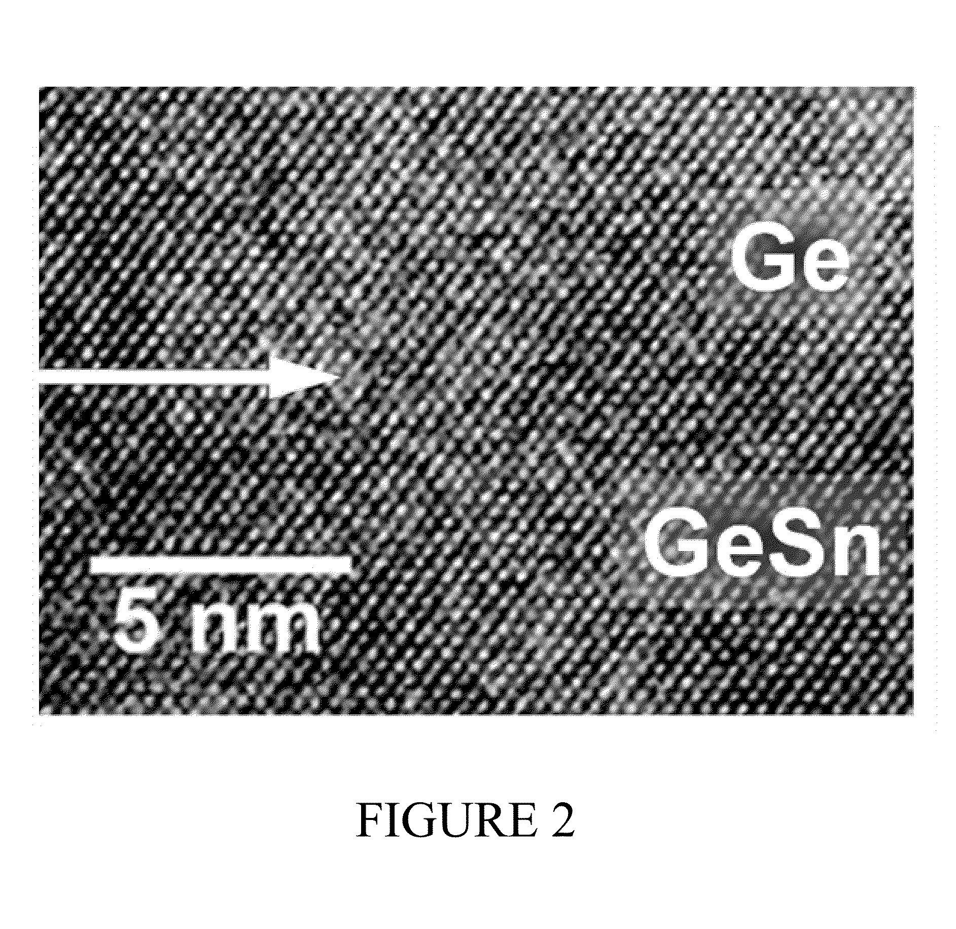
[0050]Prior to Ge growth, the Ge1-ySny / ...

example 2

Structural and Optical Characterization

[0053]The samples prepared according to Example 1 were extensively characterized for morphology, microstructure, purity and crystallographic properties by atomic force microscopy (AFM), Rutherford backscattering (RBS), secondary ion mass spectrometry (SIMS), cross sectional transmission electron microscopy (XTEM) and high resolution x-ray diffraction (XRD). The threading defects densities were estimated using an etch pit technique (EPD).

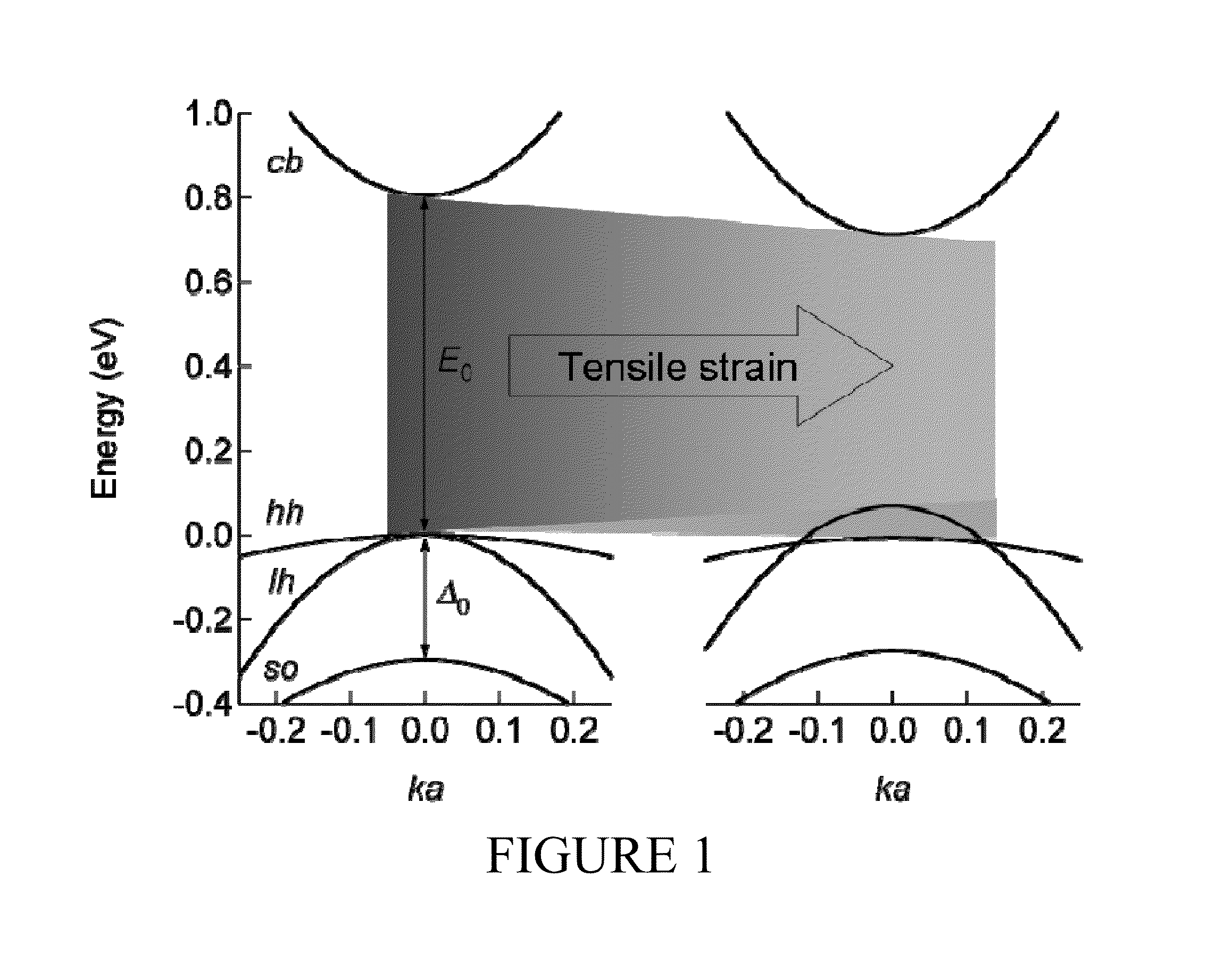
[0054]As detailed below, the precise strain state of the Ge epilayers case can be systematically manipulated by varying the thickness and composition of the underlying template, for example, via tuning of the Sn content in the Ge1-ySny buffer. Growth of Ge layers on buffers with smaller / larger lattice constants, such as Ge1-ySny with y=0.015-0.035,) systematically produced larger strains in the Ge overlayers with increasing y, within the 1.5-3.5% range.

[0055]We have used the Ge1-ySny buffer layers (y=0.015-0.035...


PUM

PropertyMeasurementUnit
tensile strainaaaaaaaaaa
band gap E0aaaaaaaaaa

Abstract

The present disclosure describes methods for preparing semiconductor structures, comprising forming a Ge1-ySny buffer layer on a semiconductor substrate and forming a tensile strained Ge layer on the Ge1-ySny buffer layer using an admixture of (GeH3)2CH2 and Ge2H6 in a ratio of between 1:10 and 1:30. The disclosure further provides semiconductor structures having highly strained Ge epilayers (e.g., between about 0.15% and 0.45%) as well as compositions comprising an admixture of (GeH3)2CH2 and Ge2H6 in a ratio of between about 1:10 and 1:30. The methods herein provide, and the semiconductor structure provide, Ge epilayers having high strain levels which can be useful in semiconductor devices for example, in optical fiber communications devices.

Description

CROSS-REFERENCE TO RELATED APPLICATIONS[0001]This application is a Divisional of U.S. patent application Ser. No. 12 / 133,221, filed Jun. 4, 2008 which claims the benefit under 35 USC §119(e), of U.S. Provisional Application Ser. No. 60 / 933,013, filed 4 Jun. 2007, which is hereby incorporated by reference in its entirety.STATEMENT OF GOVERNMENT INTEREST[0002]The invention described herein was made in part with government support under grant number FA9550-06-01-0442, awarded by AFOSR under the MURI; and under grant number DMR-0526734, awarded by the National Science Foundation. The United States Government has certain rights in the invention.BACKGROUND OF THE INVENTION[0003]Germanium has a direct band gap E0=0.81 eV at room temperature (see, MacFarlane and Roberts, Phys. Rev. 97, 1714 (1955)), which corresponds to an optical wavelength of 1.54 μm. Although this is barely enough to reach the telecom C-band (1.53 μm-1.56 μm), the very strong wavelength dependence of the absorption coeff...

Claims


Application Information

Patent Timeline
Patent Type & Authority Applications(United States)
IPC IPC(8): H01L29/12
CPCH01L21/02381H01L21/0245H01L21/02452H01L21/02631H01L21/02532H01L21/0262H01L21/0251
Inventor KOUVETAKIS, JOHNFANG, YAN-YAN
Owner ARIZONA STATE UNIVERSITY
Why Eureka
Try Eureka