Eureka AIR delivers breakthrough ideas for toughest innovation challenges, trusted by R&D personnel around the world.

Active Matrix OLED Displays and Driver Therefor

a technology of active matrix and driver circuit, which is applied in the direction of instruments, semiconductor devices, computing, etc., can solve the problems of voltage driven pixel circuit, difficult to predict the brightness of a pixel, and similar problems

Inactive Publication Date: 2011-07-28
CAMBRIDGE DISPLAY TECH LTD
View PDF8 Cites 14 Cited by
  • Summary
  • Abstract
  • Description
  • Claims
  • Application Information

AI Technical Summary

Benefits of technology

[0013]The inventors have recognised that fabricating an asymmetric select transistor, in particular with a curved gate region, the capacitance on one side of the select transistor may be decreased at the expense of increasing the capacitance on the other side of the transistor. However in the context of an active matrix pixel circuit this provides an overall performance gain since it is the input capacitance which primarily determines the programming time and thus by reducing the input capacitance of the switch / select transistor, even though the capacitance on the other side of this transistor may be increased, overall the programming time may be reduced. In embodiments the second terminal, which is coupled to the data line, comprises the source / drain region with the smaller area of overlap with the gate region.
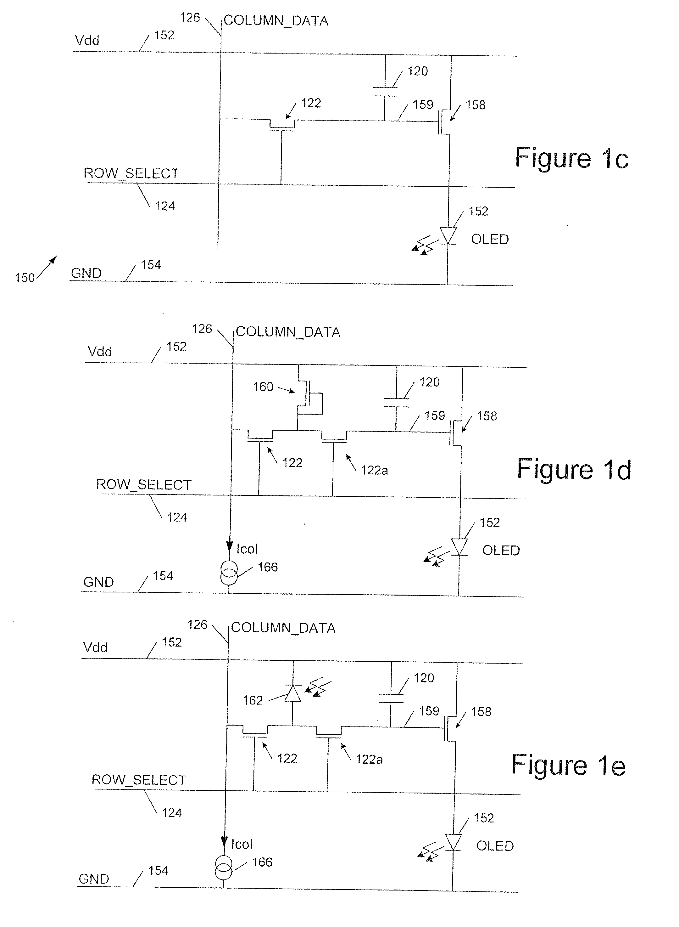
[0017]In embodiments of the pixel driver circuit with at least one further transistor (apart from the select transistor and the drive transistor) the ability to change a ratio of capacitance between the gate terminal and the two drain / source terminals can provide an additional degree of design freedom. Thus typically in programming a pixel circuit there are voltage swings within the circuit and the internal capacitances of the transistors within the circuit may be adjusted to control these—in effect a designer has some ability to choose values for the internal or “stray” capacitances within the pixel circuit.

Problems solved by technology

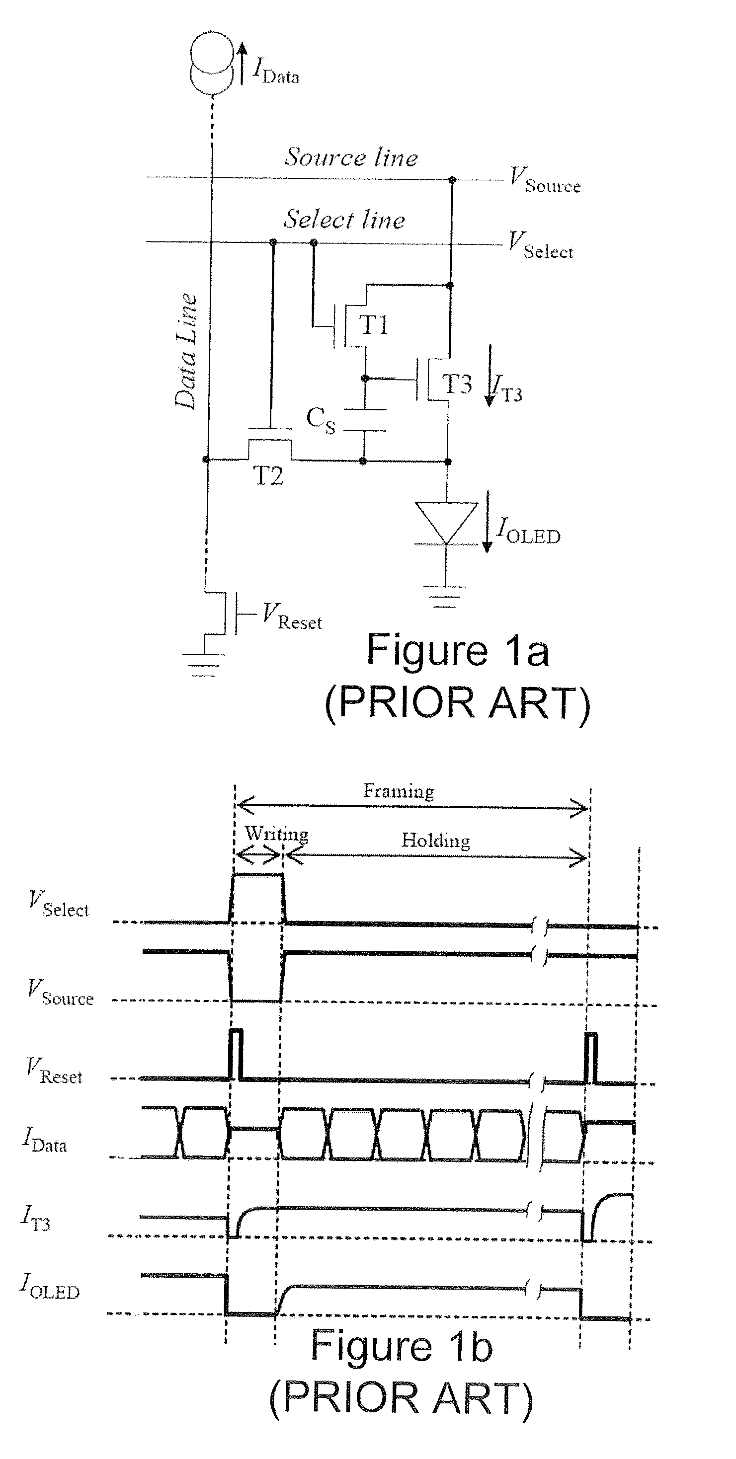
It is common to provide a current-programmed drive to an OLED because the brightness of an OLED is determined by the current flowing through the device, this determining the number of photons it generates, whereas in a simple voltage-programmed configuration it can be difficult to predict how bright a pixel will appear when driven.
Voltage driven pixel circuits, which also have a switch / stroke select transistor, exhibit similar problems.
It might be imagined that the width-to-length ratio of the switch / select transistor could be increased to decrease the resistance of this transistor and hence decrease the programming time, but this has the undesired side effect of increasing the input capacitance of this transistor which tends to work against the desired reduction in programming time.

Method used


Image

  • Active Matrix OLED Displays and Driver Therefor
  • Active Matrix OLED Displays and Driver Therefor
  • Active Matrix OLED Displays and Driver Therefor

Examples


Embodiment Construction

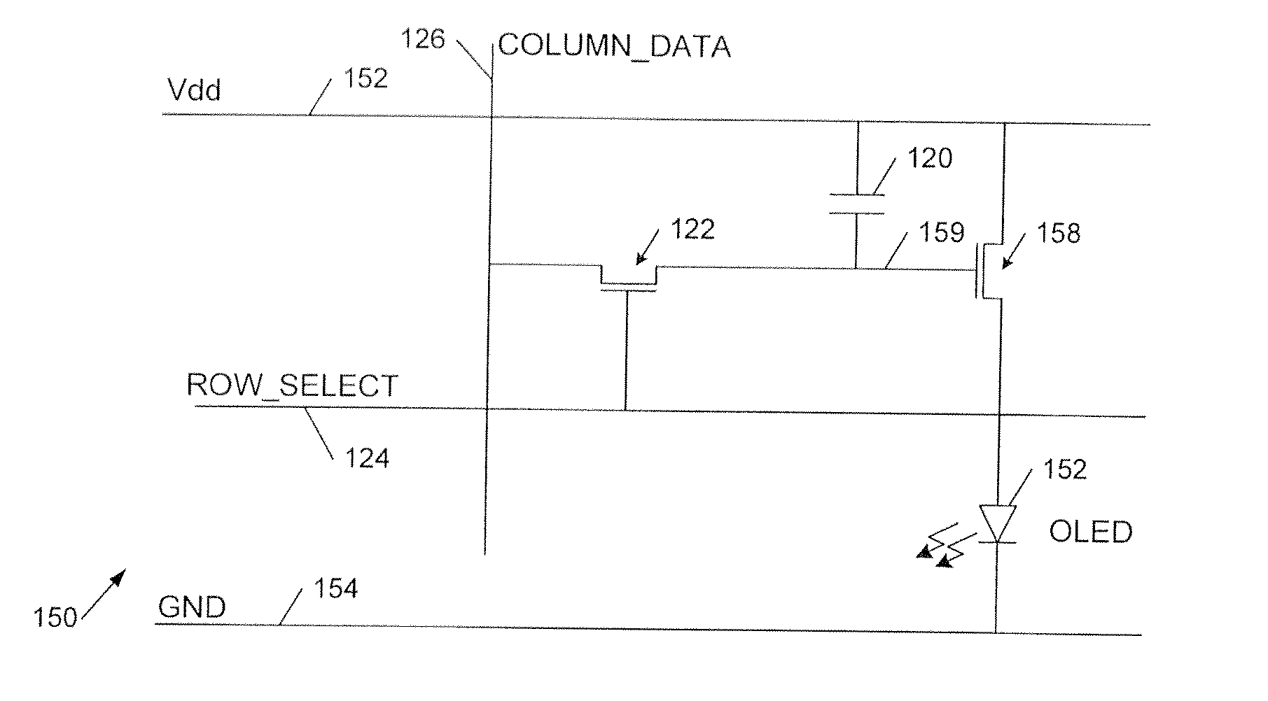
[0032]We will describe the use of an asymmetric thin film transistor (TFT) structure for the reduction of data line capacitance. The use of a curved, for example semi-circular, channel transistor enables the preferential reduction of the capacitance between the gate and one of the source / drain terminals of the transistor. Incorporating such a curved channel device into the pixel circuit of an active matrix OLED display enables improved pixel circuits to be designed. For example in the case of a select TFT connected to a programming data line on a TFT display backplane the programming time for an OLED pixel may be reduced. In embodiments the curved channel reduces the gate-contact capacitance on the inner radius whilst allowing the gate-contact capacitance on the outer radius to increase, without substantially changing the DC device performance.

Active Matrix Pixel Circuits

[0033]FIG. 1c shows an example of a voltage programmed OLED active matrix pixel circuit 150. A circuit 150 is pro...


PUM


Abstract

A display has a plurality of organic light emitting diode (OLED) pixels each with an associated pixel driver circuit, a plurality of select lines and a plurality of data lines. Each pixel driver circuit is coupled to a select line and to a data line. The pixel driver circuit includes a drive transistor configured to drive an OLED and a select transistor having a first terminal coupled to a select line and a second terminal coupled to a data line, wherein one of the terminals of said select transistor comprises a gate connection of said select transistor and wherein the other terminal comprises one of a drain and a source connection of said select transistor, and wherein said select transistor comprises source, drain and gate regions, wherein said gate region at least partially overlaps said source and drain regions, and wherein an area of said overlap of said gate region with one of said source region and said drain region is greater than an area of said overlap with the other region so that a capacitance between said gate connection and one of said drain and source connections is less than a capacitance between said gate connection and the other connection.

Description

FIELD OF THE INVENTION[0001]This invention relates to pixel driver circuits for active matrix optoelectronic devices, in particular OLED (organic light emitting diodes) displays, and the associated displays.BACKGROUND TO THE INVENTION[0002]Embodiments of the invention will be described while particularly useful in active matrix OLED displays although applications and embodiments of the invention are not limited to such displays and may be employed with other types of active matrix display and also, in embodiments, in active matrix sensor arrays.[0003]Organic light emitting diodes, which here include organometallic LEDs, may be fabricated using materials including polymers, small molecules and dendrimers, in a range of colours which depend upon the materials employed. Examples of polymer-based organic LEDs are described in WO 90 / 13148, WO 95 / 06400 and WO 99 / 48160; examples of dendrimer-based materials are described in WO 99 / 21935 and WO 02 / 067343; and examples of so called small mole...

Claims


Application Information

Patent Timeline
IPC IPC(8): G09G3/30G06F3/038
CPCH01L27/124H01L29/41733G09G3/3225H10K59/12H01L27/12H01L27/1214
Inventor SMITH, EUAN C.
Owner CAMBRIDGE DISPLAY TECH LTD
Why Eureka
Eureka Blog
Learn More