
Lithography system with lens rotation

Inactive Publication Date: 2011-07-21
ASML NETHERLANDS BV
View PDF7 Cites 17 Cited by
  • Summary
  • Abstract
  • Description
  • Claims
  • Application Information

AI Technical Summary

Benefits of technology

[0023]A further advantage of the invention holds that the stroke needed to position the projection lens accurately is significantly smaller compared to the positioning of the chuck with regard to the base frame, as would otherwise be performed in the wafer stage. It has in accordance with yet a further insight been realized that this small stroke of the projection lens allows the use of piezo-actuators rather than Lorentz motors as are known from prior art embodiments. Piezo-actuators have the advantage of not emitting electromagnetic dispersion fields which is highly desirable in charged particle lithography systems, reducing the need for complicated electromagnetic shielding.
[0024]By performing the positioning in the plane of the projection lens and the target, i.e. perpendicular to the optical axis, using actuation and positioning of the projector with regard to the metro frame, the long stroke measurement system is significantly simplified. The accuracy requirements on the chuck and wafer stage are thus lowered significantly. The projector now only has to account for the relative small errors of the short stroke enabling the use of a capacitive measurement system of relative simplicity.
[0025]The present invention also offers the ability to perform adjustments for alignment errors in the charged particle system. During assembly of a charged particle column, great care has to be taken to correctly align the components comprising the charged particle system correctly with respect to one another. In particular this is necessary for the projector, where several components such as the deflection plates that comprise the electrostatic lens are positioned with relatively high accuracy within 500 nm of their required positions. Other components in the charged particle system that are involved in the final projection of the image on the target are positioned with micrometer accuracy. Given these high accuracy requirements of the charged particle exposure system in general and the projector in particular, this necessary alignment of components is both costly and time consuming. The reduction of alignment requirements as realized by the present invention by being able to compensate for both rotational errors and errors in the Z-direction using one or more degrees of freedom is not only highly desirable in view of advancing technology nodes, but also for use in the current technology node.
[0026]A further advantage of performing part of the positioning actions using the projector is to account for rotational errors resulting from the wafer positioning system. This, combined with the previous advantage, reduces the overall requirements on the measurement system of the lithography system with regard to rotational errors, in fact to the same order of magnitude of the other requirements which is highly desirable for manufacturing.
[0027]The present invention further recognizes that the masses that have to be moved and positioned in the projector of a charged particle column are much lower as compared to the combined masses of the stage, chuck and wafer, thereby reducing the load on the control system, thus taking advantage of the fact that the mass of the projector is much lower as compared to a wafer positioning system. This is especially true in the case of high frequency motions, i.e. high speed motions. Thus, the present inventions lowering of the moving mass, enables the ability to use higher speed motions, which in turn allows the manufacturing output, i.e. the number of wafers processed per hour, to be increased.
[0028]A further insight underlying the present invention is that such inclusion of part of the required positioning can very well be performed simple and cost effective. In the latter respect e.g. a combination of a few of piezo-actuators with spring elements and capacitive sensors may be used for realizing the same. Such actuators, spring elements and sensors are generally known, widely available and not unduly costly.

Problems solved by technology

In this process very high accuracy is of prime importance, implying complex and expensive actuation and positioning means.
Therefore, for as far as known in the art, most maskless lithography systems are combined with a stage of relatively simple design, i.e. having the disadvantage of low throughput and / or limited functionality.
A further complication towards successful exposure lies in the fact that while the known charged particle system has means to compensate for errors in the XY-plane of the target using the deflection in the writing direction and the movement of the target holder, it is unable to correct for rotational errors using said deflection and movement of the target holder.
Said rotational errors, originating from misalignment around the Z-axis of the projection system and target, in fact from insufficient accuracy in the guidance of the stage in the X- and Y-direction respectively, ultimately result in a position error with this effect being increased when projection takes place further away from the centre of rotation, thereby increasing the accuracy requirements with regard to rotational errors for the target positioning system even further.
These known positioning systems, for as far as they can be adapted to maskless lithography, are mostly inappropriate for use in a maskless lithography system at least in the sense of e.g. size, costs and vacuum compatibility.
Also, electromagnetic dispersion fields as commonly present at actuators, in particular electromagnetic actuators such as Lorentz motors, are normally undesirable in charged particle projection systems since these electromagnetic fields negatively influence the quality of exposure.
When used, electromagnetic actuators invariably necessitate complex magnetic shielding, increasing the complexity and cost of the maskless lithography system.
Where embodiments of positioning systems are disclosed in combination with charged particle exposure systems, they are up to now of a conceptual or relatively expensive nature, suited for prototyping purposes, rather than for large scale manufacture.
Said measurement system, also referred to as metrology system, represents an expensive part of the wafer positioning system in commercially available lithography systems.
In this system many features are to be duplicated, implying a technically complicated and costly solution.
As charged particle beam systems, in general maskless systems, by their nature have a relatively low manufacturing output; this increased complexity brought on by high wafer throughput in optical lithography is not necessary and actually unwanted.
Combination of at least this known industrial target stages with modern charged particle beam systems, in particular maskless lithography systems is thus undesired.
Another disadvantage of this known system is that it offers no means for adjusting in the Z-direction and is therefore unable to correct errors in the Z-direction, for instance errors due to thickness variations of the target.
However, this timing adjustment only allows for corrections in one direction, effectively having only one degree of freedom.
This method is unable to correct for errors in the Z-direction, for instance errors due to thickness variations of the target, and rotations around the Z-axis due to rotational errors.
In the latter case, the document does not teach how the adjustment in the Z-direction may be achieved.
This known approach does not allow for the compensation of rotational errors around the Z-axis, which are technically more challenging to achieve, especially in a multiple beam charged particle system.
Measurement and control systems of this type are typically costly, increasing the total cost of the lithographic apparatus.
A further disadvantage of this known system is that it uses Lorentz motors for actuation implying electromagnetic dispersion fields.
Therefore this feature complicates if not prohibits any combination of this known target positioning system with a charged particle beam lithography system as presently at stake.

Method used


Image

  • Lithography system with lens rotation
  • Lithography system with lens rotation
  • Lithography system with lens rotation

Examples


Embodiment Construction

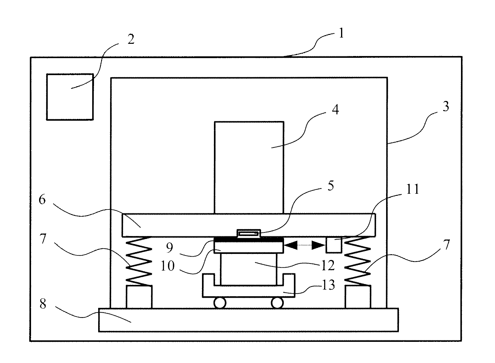
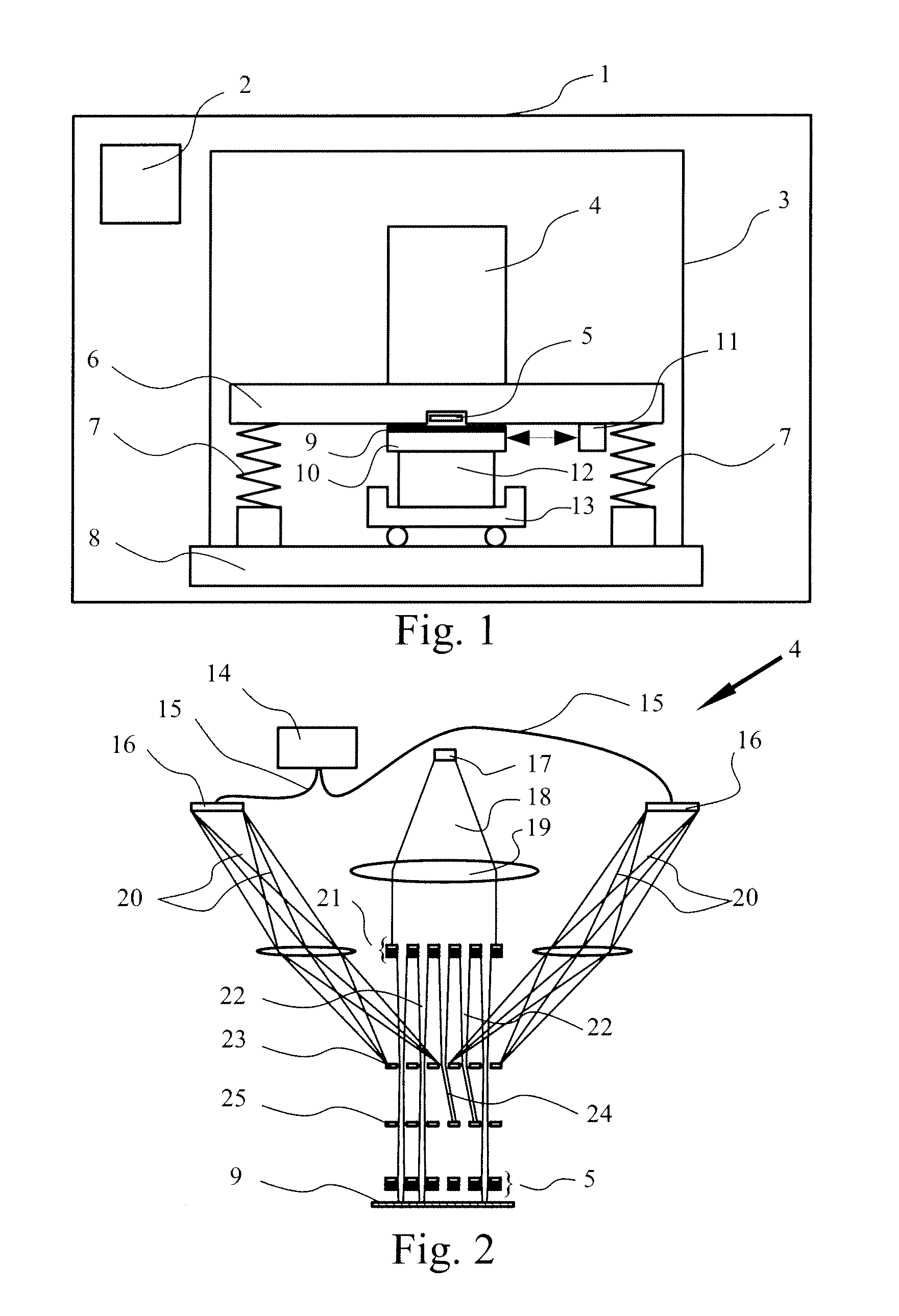
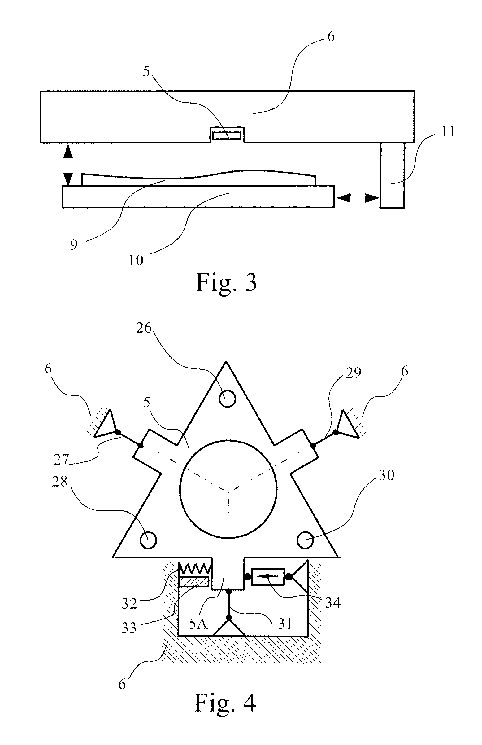
[0069]FIG. 1 is a schematic representation of a prior art charged particle system 1 for projecting an image, in particular a control system provided image, onto a target. It includes the wafer stage components to which part of the present invention relates in particular. In this design the charged particle system comprises a control system 2, a vacuum chamber 3 mounted on the base frame 8, which contains the charged particle column 4, the metro frame 6 and the target positioning system 9-13. Said target 9 will generally be a wafer provided with a charged particle sensitive layer in the substrate plane. Target 9 is placed on top of wafer table 10, which is in turn placed on chuck and long stroke drive 13. Measurement system 11 is connected to metrology frame 6 and provides measurements of the relative positioning of wafer table 10 and metro frame 6. The metro frame 6 typically is of relatively high mass and is suspended by vibration isolators 7 for example embodied by spring elements...


PUM


Abstract

The invention relates to a charged particle based lithography system for projecting an image on a target using a plurality of charged particle beamlets for transferring said image to said target, said system comprising a charged particle column comprising:an electron optical subassembly comprising a charged particle source, a collimator lens, an aperture array, a blanking means and a beamstop for generating a plurality of charged particle beamlets; anda projector for projecting said plurality of charged particle beamlets on said target;said projector being moveably included in the system by means of at least one projector actuator for moving said projector relative to said electron optical subassembly;said projector actuator being included for mechanically actuating said projector and providing said projector with at least one degree of freedom of movement;wherein said degree of freedom relates to a movement around an optical axis of the system.

Description

BACKGROUND OF THE INVENTION[0001]1. Field of the Invention[0002]The present invention relates to a charged particle based lithography system for projecting an image on a target such as a wafer, using a plurality of beamlets for transferring said image to said target, said system comprising a projector for projecting a plurality of beamlets on said target, and at least one actuator for positioning said projected image and said target relative to one another.[0003]2. Description of the Related Art[0004]Such systems are generally known and have the advantage of fabrication on demand and possibly lower tool cost, due to a lack in necessity to use, change and install masks. One example of such a system, disclosed in WO2007 / 013802, comprises a charged particle column operating in vacuum with a charged particle source including a charged particle extraction means, a means for creating a plurality of parallel beamlets from said extracted charged particles and a plurality of electrostatic le...

Claims


Application Information

Patent Timeline
IPC IPC(8): H01J3/14H01J3/22H01J3/18
CPCB82Y10/00B82Y40/00H01J2237/1502H01J37/10H01J37/3177H01J37/023H01J37/317H01J37/20H01J37/22
Inventor PEIJSTER, JERRY
Owner ASML NETHERLANDS BV
Learn More