Trace detection device of biological and chemical analytes and detection method applying the same
a detection device and biological and chemical analyte technology, applied in the direction of optical radiation measurement, semiconductor/solid-state device testing/measurement, instruments, etc., can solve the problems of limiting its timeliness and popularity, limiting the intensity of raman scattering, and high cost of mass spectrometry
- Summary
- Abstract
- Description
- Claims
- Application Information
AI Technical Summary
Problems solved by technology
Method used
Image


Examples
example 1
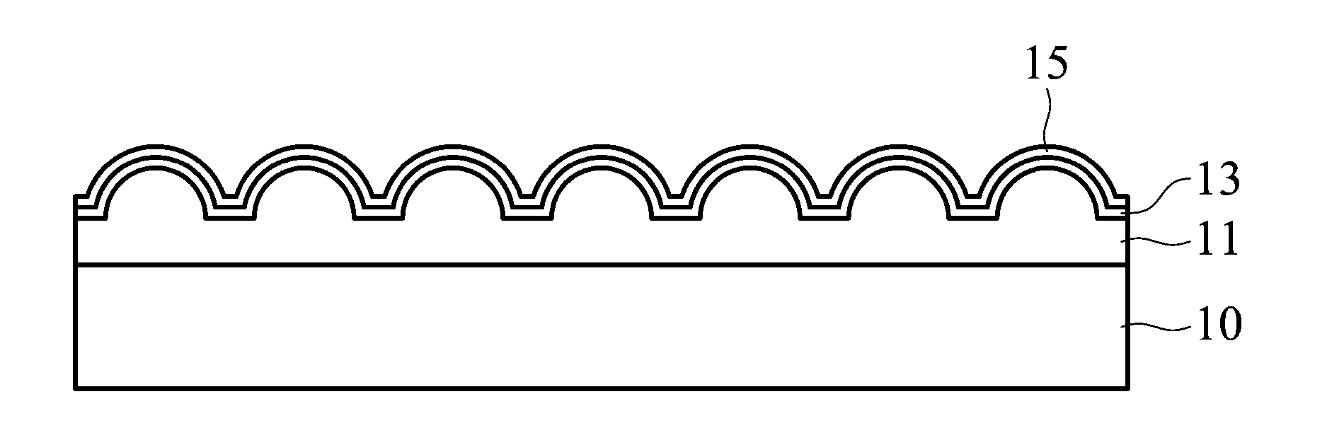
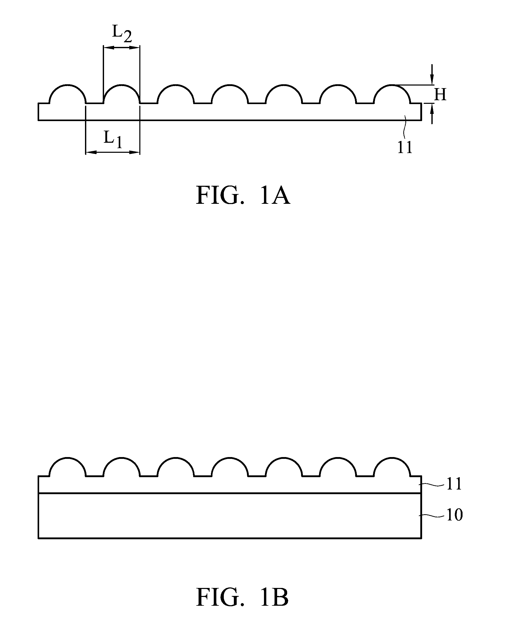
[0031]A periodic nickel nanostructure was formed by nanoimprint, and then transformed on a nickel substrate by electroless plating. The periodic nickel nanostructure had a shape of a sine wave, a period (L1) of 300 nm, a width (L2) of 150 nm, and a height (H) of 150 nm, wherein the aspect ratio (H / L2) is 1. 400 nm of silicon dioxide layer was then conformably formed on the periodic nickel nano structure by chemical vapor deposition, and 20 nm of continuous silver film was then conformably formed on the silicon dioxide layer by sputtering. As such, the continuous silver film was formed on the nickel substrate, and the silicon dioxide layer is disposed therebetween. The described device was charged in different mediums such as air and water to measure its absorption ratio versus different wavelengths. As shown in the dotted circle 21 of FIG. 2, when the device was moved from water having higher refractive index to air having lower refractive index, its surface plasmon resonance absorp...
example 2
[0035]Similar to Example 1, the difference was that the continuous silver film thickness thickened from 20 nm to 25 nm in Example 2, other periodic nickel nanostructure factors and the silicon dioxide layer thickness were same. The devices of Examples 1 and 2 were charged in water to measure their absorptions versus different wavelength. As shown in the dotted circle 51 in FIG. 3, the surface plasmon resonance absorption peak wavelength of the device having thicker continuous silver film in Example 2 was blue shifted compared to the device in Example 1. In addition, the dotted circles 53 showed the absorption peaks caused by thin film interference of the metal-dielectric-metal sandwich structure.
[0036]As described above, the absorption peak wavelength of the device could be tuned to coincide with the incident laser wavelength by changing the continuous metal film thickness on the same periodic nanostructure.
example 3
[0037]Four periodic nickel nanostructures as described in Example 1 were provided, and 50 nm, 100 nm, 150 nm, and 200 nm of silicon dioxide layers were conformably formed on the different periodic nickel nanostructures by chemical vapor deposition, respectively. Subsequently, 25 nm continuous silver films are conformably formed on the silicon dioxide layers, respectively by sputtering, such that the devices having the periodic nanostructures, the continuous silver films, and the silicon dioxide layer having different thickness therebetween were obtained. The devices of Example 3 were charged in different mediums such as air and water to measure their absorption peaks due to surface plasmon resonance. As shown in FIG. 6, the surface plasmon resonance absorption peak wavelength of the devices was red shifted by thickening the dielectric layer, it meant that the surface plasmon resonance absorption peak wavelength could be tuned by changing the dielectric layer thickness. In addition, ...
PUM
| Property | Measurement | Unit |
|---|---|---|
| thickness | aaaaa | aaaaa |
| refractive index | aaaaa | aaaaa |
| refractive index | aaaaa | aaaaa |
Abstract
Description
Claims
Application Information
 - R&D
- Intellectual Property
- Life Sciences
- Materials
- Tech Scout
- Unparalleled Data Quality
- Higher Quality Content
- 60% Fewer Hallucinations
Browse by: Latest US Patents, China's latest patents, Technical Efficacy Thesaurus, Application Domain, Technology Topic, Popular Technical Reports.
© 2025 PatSnap. All rights reserved.Legal|Privacy policy|Modern Slavery Act Transparency Statement|Sitemap|About US| Contact US: help@patsnap.com