Method for manufacturing bonded wafer
a technology of bonded wafers and thin films, applied in the direction of semiconductor/solid-state device manufacturing, basic electric elements, electric apparatus, etc., can solve the problems of increasing the thickness of buried insulator films (boxes), and increasing the number of defects, so as to reduce the defect generation of thin films of a variety of bonded wafers and reduce the number of defects. , the effect of particle reduction
- Summary
- Abstract
- Description
- Claims
- Application Information
AI Technical Summary
Benefits of technology
Problems solved by technology
Method used
Image

Examples
example 1
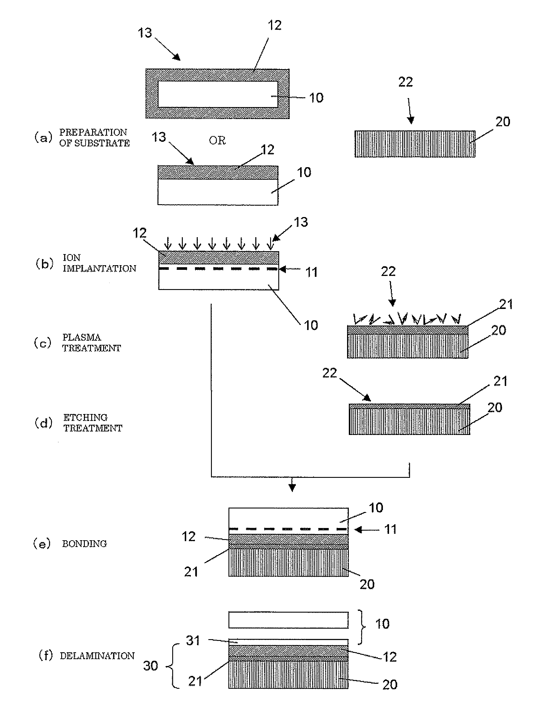
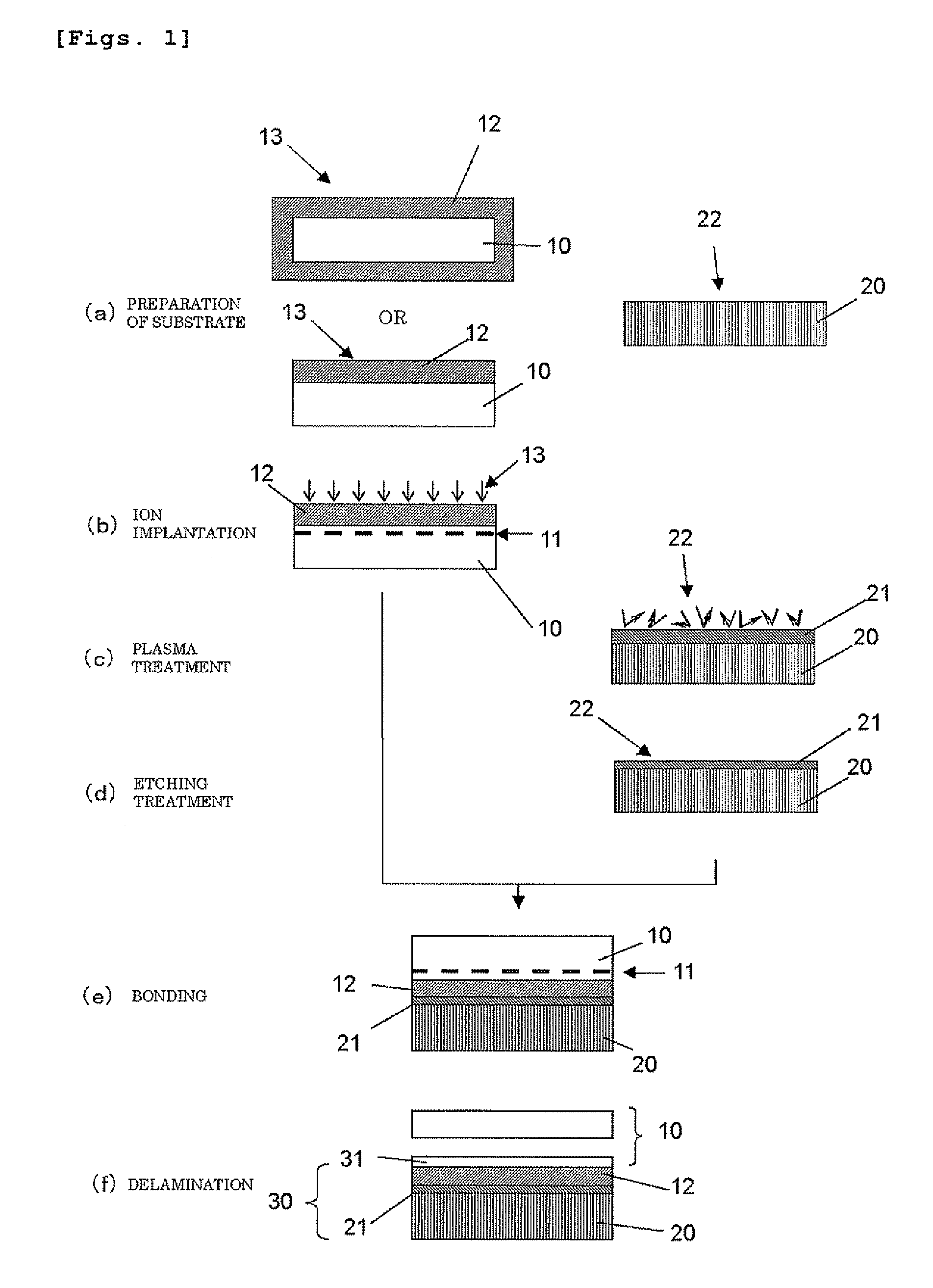
[0045]Two mirror-polished silicon single crystal wafers each having a diameter of 300 mm were prepared as a bond wafer and a base wafer, a thermal oxide film having a film thickness of 20 nm was formed on a surface of the bond wafer as an insulator film. Subsequently, a hydrogen ion was implanted through the thermal oxide film on the bond wafer under conditions of 50 keV and 6×10¹⁶ / cm2 to form an ion-implanted layer.
[0046]Then, a nitrogen plasma treatment (a room temperature, a gas flow rate of 115 sccm, a pressure of 0.4 Torr (53.3 Pa), an output of 100 W, and 15 seconds) was applied to the surface of the oxide film on the bond wafer and a silicon single crystal surface (where approximately 1 nm of a natural oxide film is formed) of the base wafer. As a result, a film thickness of the oxide film on the bond wafer was 21 nm, and a film thickness of the oxide film on the base wafer was 4 nm.
[0047]Subsequently, the wafers subjected to the plasma treatment were immersed in an SC1 clean...
examples 2 to 5
, Comparative Examples 1 to 4
[0049]A bond wafer (having a 20 nm of a thermal oxide film and hydrogen ion implantation performed thereto) and a base wafer (having 1 nm of a natural oxide film) equal to those in Example 1 were prepared, a nitrogen plasma treatment and an oxide film etching treatment under the same conditions as those in Example 1 were carried out or not carried out in various combinations depicted in Table 1, and the number of defects generated in a silicon thin film of a bonded wafer was measured like Example 1. Table 1 shows a measurement result.
TABLE 1BOND WAFERBASE WAFER(WITH INSULATOR FILM)(WITHOUT INSULATOR FILM)NUMBER OFPLASMAETCHINGPLASMAETCHINGDEFECTSEXAMPLE 1APPLIEDAPPLIEDAPPLIEDAPPLIED5EXAMPLE 2APPLIEDAPPLIEDAPPLIEDNONE10EXAMPLE 3APPLIEDAPPLIEDNONENONE16EXAMPLE 4APPLIEDNONEAPPLIEDAPPLIED10EXAMPLE 5NONENONEAPPLIEDAPPLIED1COMPARATIVEAPPLIEDNONEAPPLIEDNONE141EXAMPLE 1COMPARATIVEAPPLIEDNONENONENONE137EXAMPLE 2COMPARATIVENONENONEAPPLIEDNONE125EXAMPLE 3COMPARATIV...
example 6
[0054]Two mirror-polished silicon single crystal wafers each having a diameter of 300 mm were prepared as a bond wafer and a base wafer, and a thermal oxide film having a thickness of 20 nm was formed as an insulator film on a surface of each of the bond wafer and the base wafer. Subsequently, a hydrogen ion was implanted through the thermal oxide film on the bond wafer under conditions of 50 keV and 6×10¹⁶ / cm2 to form an ion-implanted layer.
[0055]Then, a nitrogen plasma treatment was applied to surfaces of the oxide films on both the wafers under the same conditions as those in Example 1, both the wafers subjected to the plasma treatment were immersed in an SC1 cleaning liquid and an SC2 cleaning liquid, and a liquid temperature and an immersion time were adjusted, thereby etching each oxide film to reduce its film thickness by 2 nm.
[0056]After the oxide film etching treatment, a bonded wafer was fabricated under the same conditions as those in Example 1, a silicon thin film of thi...
PUM
 Abstract
Description
Claims
Application Information
 - R&D
- Intellectual Property
- Life Sciences
- Materials
- Tech Scout
- Unparalleled Data Quality
- Higher Quality Content
- 60% Fewer Hallucinations
Browse by: Latest US Patents, China's latest patents, Technical Efficacy Thesaurus, Application Domain, Technology Topic, Popular Technical Reports.
© 2025 PatSnap. All rights reserved.Legal|Privacy policy|Modern Slavery Act Transparency Statement|Sitemap|About US| Contact US: help@patsnap.com