
Rapid Growth Method and Structures for Gallium and Nitrogen Containing Ultra-Thin Epitaxial Structures for Devices

a gallium and nitrogen technology, applied in the field of lighting techniques, can solve the problems of conventional edison light bulbs, low light intensity, and low light intensity, and achieve the effect of rapid growth of gallium

Inactive Publication Date: 2011-03-10
SORAA
View PDF104 Cites 236 Cited by
  • Summary
  • Abstract
  • Description
  • Claims
  • Application Information

AI Technical Summary

Benefits of technology

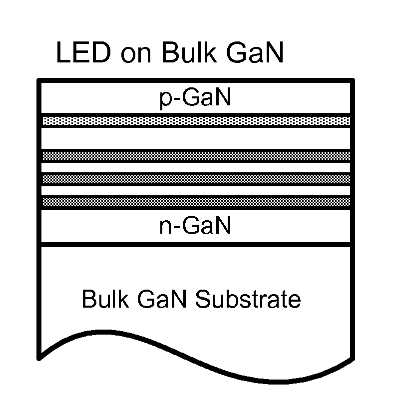
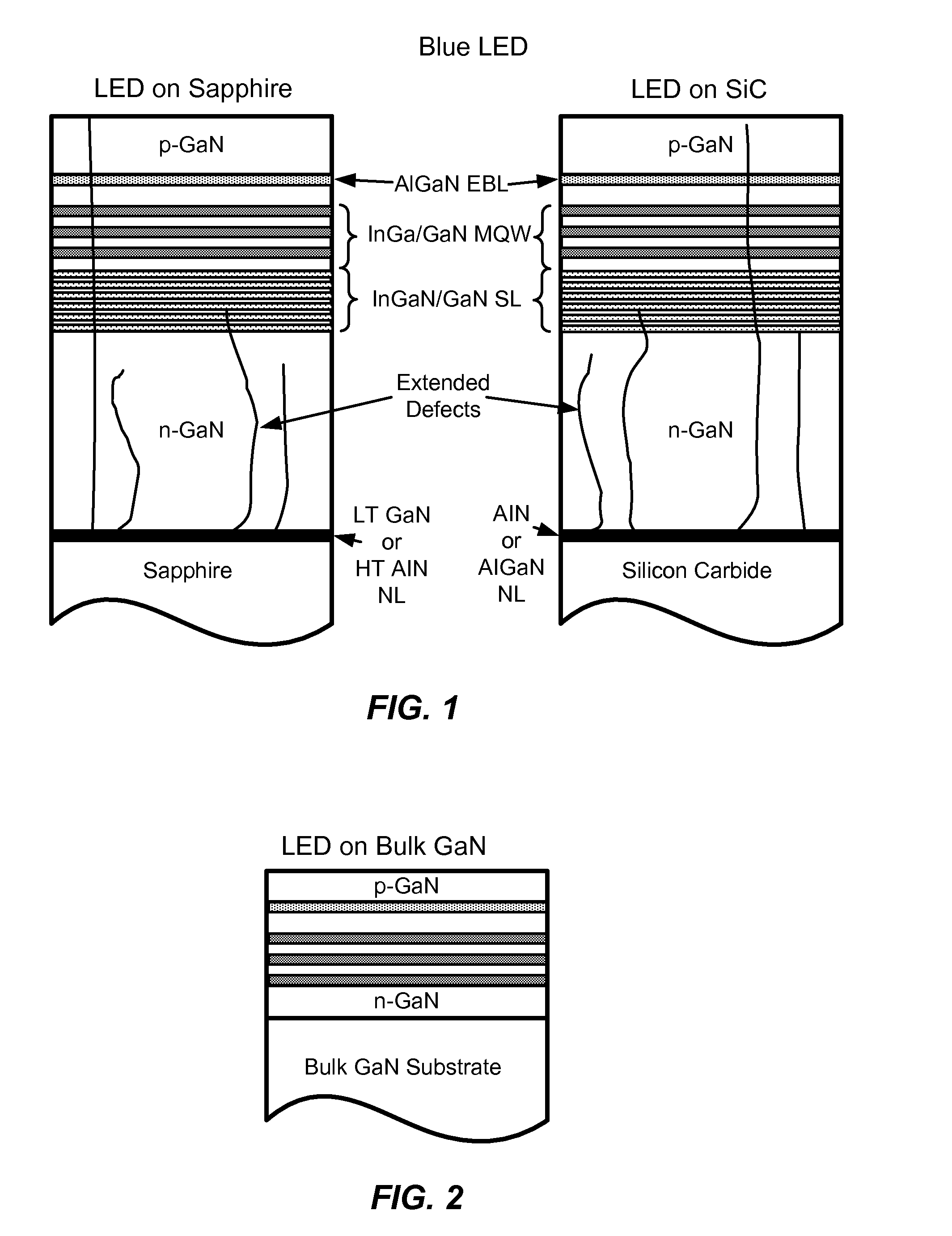
[0008]In a specific embodiment, the present invention provides a method for rapid growth of gallium and nitrogen containing material. The method includes providing a bulk gallium and nitrogen containing substrate having a surface region. The method forms a first epitaxial material of first thickness over the surface of the bulk gallium and nitrogen containing substrate. In a preferred embodiment, the first epitaxial material is pseudomorphically formed. The method also forms second epitaxial material over the first epitaxial material to form a stacked structure. In a preferred embodiment, the second epitaxial materials form an active region, e.g., a junction. Preferably, the stacked structure has a total thickness of less than about 2 microns and characterizes at least substantial portion of an epitaxial region of an optical or electrical device. As used herein, the terms “first” and “second do not generally imply any order or sequence. In a specific embodiment, “pseudomorphically” generally means a lattice matched process where the first epitaxial material is latticed matched to the bulk gallium and nitrogen containing substrate. In a preferred embodiment, the epitaxially formed gallium nitride material and bulk gallium and nitrogen containing substrate has an interface that is substantially or completely latticed matched with each other.
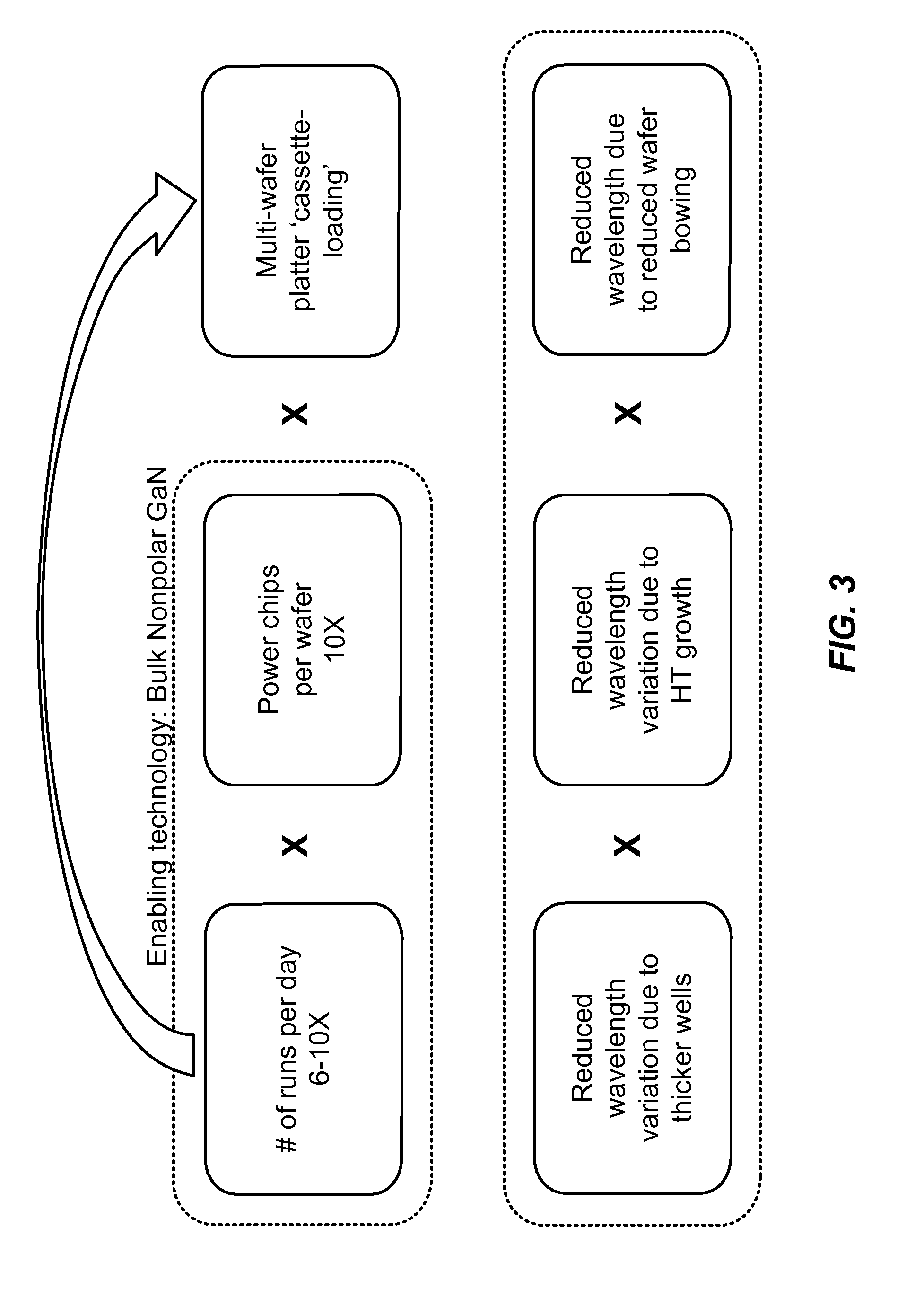
[0011]In another embodiment, the epitaxial material or materials can be formed in a reactor that can handle multiple wafers in an automatic growth sequence such as an autocassettes. In such a configuration, the wafer loading and unloading from the growth chamber to the loadlock can be performed automatically, without interruption or waiting for wafer transfer between the loadlock and the laboratory or production floor. One configuration uses robotic arms to transfer wafers between the loadlock chamber and the reaction chamber. In such a configuration, the wafers are transferred to and from the growth chamber on a susceptor or tray, on which the wafer will be subjected to epitaxial growth. In a preferred embodiment, the susceptor or tray will contain multiple wafers such that epitaxial material or materials can be formed in a reactor chamber and be grown on multiple wafers at the same time. As used herein, the term auto-cassette generally means a cassette having a sequence of trays, each of which has a substrate wafer or work-piece, that allow for automatic loading of each work piece in a sequential manner. In a preferred embodiment, the cassette including multiple substrates or work-pieces is maintained in a chamber, which couples to the MOCVD chamber, and therefore reduces handling time and the like.
[0013]The present invention provides a method for rapid growth of gallium and nitrogen containing material. The method includes providing a bulk gallium and nitrogen containing substrate having a surface region and forming a first epitaxial material having a first thickness at a growth rate of at least 4 nm per hour overlying the surface region of the bulk gallium and nitrogen containing substrate. The first epitaxial material is pseudomorphically formed overlying the surface region of the bulk gallium and nitrogen containing substrate. The method includes forming one or more second epitaxial materials overlying the first epitaxial material and configured to form a stacked structure.
[0015]The method provides smooth epitaxial material. Using for example, n-type gallium and nitrogen containing material, surface roughness is characterized by about 1 nm RMS and less for a five micron by five micron spatial area. Using for example p-type gallium and nitrogen containing material, surface roughness is characterized by about 1 nm RMS and less for a five micron by five micron spatial area.

Problems solved by technology

Unfortunately, drawbacks exist with the conventional Edison light bulb.
That is, the conventional light bulb dissipates much thermal energy.
Additionally, the conventional light bulb routinely fails often due to thermal expansion and contraction of the filament element.
Other colored LEDs have also been proposed, although limitations still exist with solid state lighting.

Method used


Image

  • Rapid Growth Method and Structures for Gallium and Nitrogen Containing Ultra-Thin Epitaxial Structures for Devices
  • Rapid Growth Method and Structures for Gallium and Nitrogen Containing Ultra-Thin Epitaxial Structures for Devices
  • Rapid Growth Method and Structures for Gallium and Nitrogen Containing Ultra-Thin Epitaxial Structures for Devices

Examples


example

[0098]To prove the principle and operation of the experiment, we performed certain experiments. We demonstrated high quality GaN epitaxial films at high growth rates of 4 microns per hour and greater. The experiment was performed using an atmospheric pressure MOCVD reactor configured with reactant gases, as noted. The chamber is configured to provide thermal energy to the growth as noted. The temperature of the reaction is measured by thermo-couples coupled to the susceptor, which holds the bulk wafer. It is believed that the temperature of the growth is slightly lower than those noted herein. Additionally, the experiment was performed using the following parameters.

1. Bulk wafer:

[0099]Non-polar, semipolar, or polar

[0100]GaN based material

[0101]Threading dislocation (TD) density<1E8 cm-2

[0102]Stacking fault (SF) density<1E4 cm-1

[0103]N-type Silicon Doping>1E17cm-3

2. N type epitaxial material:

[0104]Thickness of<2 um

[0105](Al,Ga,In) N based material

[0106]950 C


PUM


Abstract

A method for rapid growth of gallium and nitrogen containing material is described. The method includes providing a bulk gallium and nitrogen containing substrate. A first epitaxial material of first thickness is formed over the substrate, preferably with a pseudomorphical process. The method also forms a second epitaxial layer over the first to create a stacked structure. The stacked structure consists of a total thickness of less than about 2 microns.

Description

CROSS-REFERENCE TO RELATED APPLICATIONS[0001]This application claims priority to U.S. Provisional Application No. 61 / 235,989 (Attorney Docket No. 027364-007500US), filed Aug. 21, 2009, commonly assigned, and hereby incorporated by reference in its entirety for all purposes.BACKGROUND OF THE INVENTION[0002]This invention relates generally to lighting techniques. More specifically, embodiments of the invention include techniques for rapid growth of epitaxial structures using Metal-Organic Chemical Vapor Deposition (“MOCVD”) technology on bulk gallium and nitrogen containing materials. The invention can be applied to applications such as white lighting, multi-colored lighting, lighting for flat panel displays and other optoelectronic devices, as well as other uses.[0003]In the late 1800's, Thomas Edison invented the light bulb. The conventional light bulb, commonly called the “Edison bulb,” has been used for over one hundred years. The conventional light bulb uses a tungsten filament e...

Claims


Application Information

Patent Timeline
IPC IPC(8): C30B25/20C30B25/02C30B25/08
CPCC30B25/02C30B29/406H01L21/02389H01L33/0075H01L21/02507H01L21/0254H01L21/0262H01L21/02458
Inventor RARING, JAMESCHAKRABORTY, ARPANPOBLENZ, CHRISTIANE
Owner SORAA
Learn More