Bipolar transistor

Active Publication Date: 2011-03-03
TEXAS INSTR INC
View PDF1 Cites 4 Cited by
  • Summary
  • Abstract
  • Description
  • Claims
  • Application Information

AI Technical Summary

Benefits of technology

[0006]Accordingly, the invention provides a bipolar transistor. The bipolar transistor according to the invention includes a collector having a base layer provided thereon. The shallow trench isolation structure and the collector moat is defined such that the collector projects from the shallow trench isolation structure adjacent the collector. In other words, the surface of the collector region (this region is also often referred to as the moat region which refers to an area of silicon free of oxide although in this embodiment it is rather a plateau than a moat) protrudes from or extends above the shallow trench isolation structure. In this way, the shallow trench isolation structure step with respect to the collector is reversed (or, in other words, the thickness of the shallow trench isolation structure is reduced beyond the level of the collector plateau). This provides that the stress between the poly base region and the single crystal epitaxial base region is reduced. Therefore defects such as dislocations are eliminated or reduced.
[0007]In one embodiment of the invention, the base layer and the poly base layer may be formed from SiGe. Further, the base layer may be single crystal SiGe, while the base poly layer will be poly SiGe. Since there is a mismatch between the SiGe base layer and the Si collector, stress is implemented especially at the interface between the SiGe base layer and the SiGe base poly, that are grown simultaneously. Because the shallow trench isolation structure further defines a step such that the collector projects from the shallow trench isolation structure adjacent to the collector in the transistor according to the invention, stress between the poly SiGe layer and the single crystal SiGe layer is reduced so that defects are minimized.
[0008]The invention also provides a method of manufacturing a bipolar transistor. The method comprises forming a shallow trench isolation structure in the collector and etching the shallow trench isolation structure. Further, the step of etching comprises defining a step in the shallow trench isolation structure such that the collector projects from the shallow trench isolation structure adjacent the collector. This means that when the base layer is deposited on the collector and the base poly is deposited on the etched shallow trench isolation structure, the base layer projects or protrudes from the collector by an amount greater than the part of the base poly that is situated adjacent to the base layer. In this way, stress between the base layer and the base poly layer is minimized, which means that defects in the transistor structure are eliminated or reduced compared to a bipolar transistor manufactured by conventional non-selective epitaxial processes. The etching step may be a wet etching step. After the etching step, SiGe can be deposited for forming the base of the transistor through epitaxial growth. SiGe may then also be deposited on the shallow trench isolation regions, where the SiGe forms a poly SiGe layer. The stress at the interface between epitaxial SiGe and poly SiGe can then be reduced.
[0011]Furthermore, the time for etching the shallow trench isolation back may also be extended. The etching time may be twice the conventional etching time ore more. Etching the shallow trench isolation structure to an amount and / or for a time in this range advantageously reduces the step height of the shallow trench isolation structure so that the collector projects from the shallow trench isolation structure by an amount that further minimizes stresses between the base layer and the gate. Therefore defects in the transistor structure are further reduced.

Problems solved by technology

However, because of the lattice mismatch between germanium and silicon, between the single crystal SiGe base layer B and the polysilicon gate regions BP, stress is induced in the epitaxial SiGe layers.
This stress can result in defects such as dislocations.

Method used


Image

  • Bipolar transistor
  • Bipolar transistor
  • Bipolar transistor

Examples


Embodiment Construction

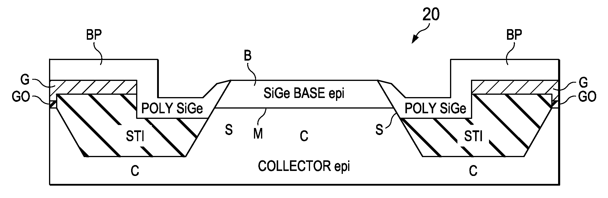
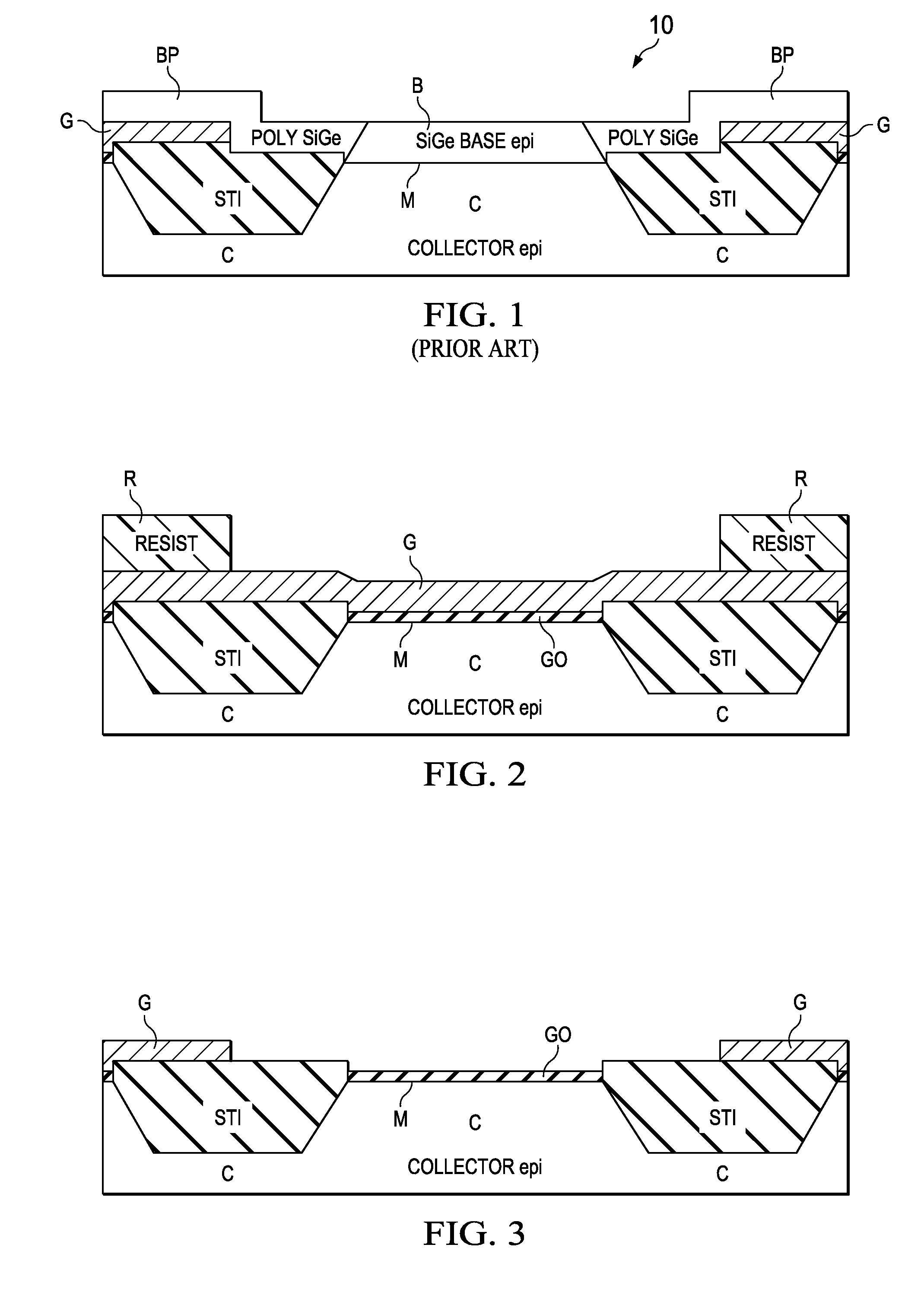
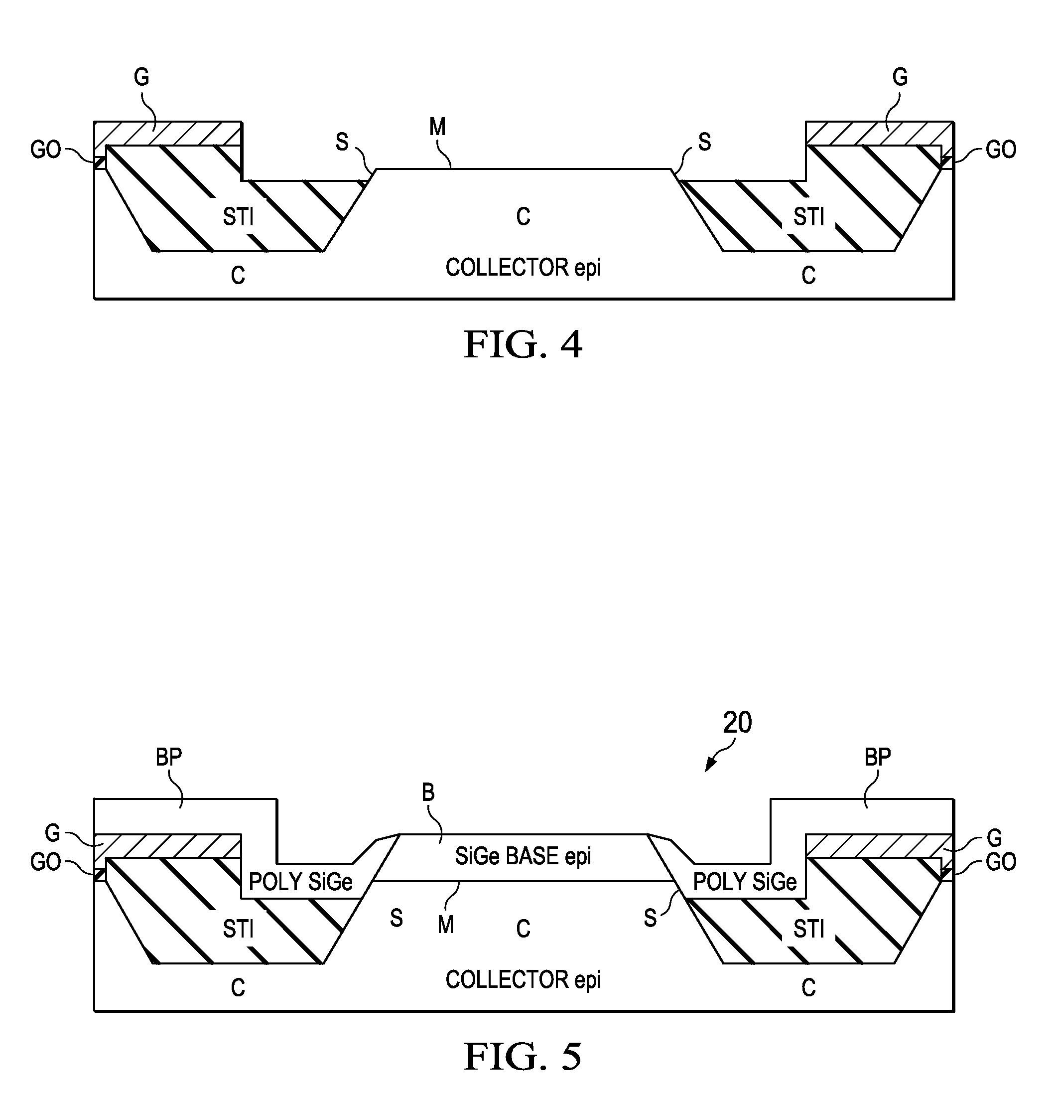
[0019]FIG. 5 shows the collector and the base regions of a bipolar transistor 20 according to the invention and FIGS. 2 to 4 are cross-sectional views at various steps in the manufacture or process flow of the bipolar transistor 20 according to the invention. Only the manufacturing steps that are applicable to the invention are described in detail in the following. Especially the fabrication of the emitter on top of the base is not described herein as it corresponds to standard processing. Although only the manufacture of an NPN transistor is shown and described here, the invention and described method of manufacture could also apply to a PNP bipolar transistor, or any bipolar transistor in a BiCMOS structure.

[0020]FIG. 2 shows a stage of manufacture of the bipolar transistor 20 after the formation of shallow trench isolation, gate oxide and gate poly deposition (gate oxide and gate poly are not part of the bipolar transistor. They are only required for the CMOS devices which are al...


PUM


Abstract

A bipolar transistor has a collector having a base layer provided thereon and a shallow trench isolation structure formed therein. A base poly layer is provided on the shallow trench isolation structure. The shallow trench isolation structure defines a step such that a surface of the collector projects from the shallow trench isolation structure adjacent the collector.

Description

FIELD OF THE INVENTION[0001]The invention generally relates to a bipolar transistor. More particularly, the invention relates to a bipolar transistor or BiCMOS structure manufactured by non-selective epitaxy and a method of manufacture thereof.BACKGROUND OF THE INVENTION[0002]The use of non-selective silicon germanium (SiGe) epitaxy is one of the key processes in modern manufacturing technologies for bipolar transistors. Non-selective epitaxy defines the electrical properties of the bipolar base and makes high speed bipolar devices possible. During this non-selective deposition, single crystal SiGe is deposited on open silicon regions while poly SiGe is grown on oxide surfaces like shallow trench isolation structures (STI).[0003]An example of an NPN transistor structure 10 manufactured by non-selective epitaxy is shown in FIG. 1. A collector C is formed as an epitaxial layer and etched so that shallow trench isolation structures STI are formed therein. After deposition of a gate pol...

Claims


Application Information

Patent Timeline
IPC IPC(8): H01L29/201H01L21/331
CPCH01L21/76232H01L29/737H01L29/66242H01L29/0649
Inventor SCHIMPF, KLAUSSCHIEKOFER, MANFREDWILLIS, CARL DAVIDWAITSCHULL, MICHAELPLOSS, WOLFGANG
Owner TEXAS INSTR INC
Why Eureka
Try Eureka