
Electrochemical etching and polishing of conductive substrates

a technology of electrochemical etching and substrate polishing, which is applied in the manufacture of electrolysis components, printed circuits, manufacturing tools, etc., can solve the problems of non-active” electrolyte solutions that do not provide chemical etching capability, and achieve the effect of minimising undercutting

Inactive Publication Date: 2011-01-27
FARADAY TECH INC
View PDF58 Cites 19 Cited by
  • Summary
  • Abstract
  • Description
  • Claims
  • Application Information

AI Technical Summary

Benefits of technology

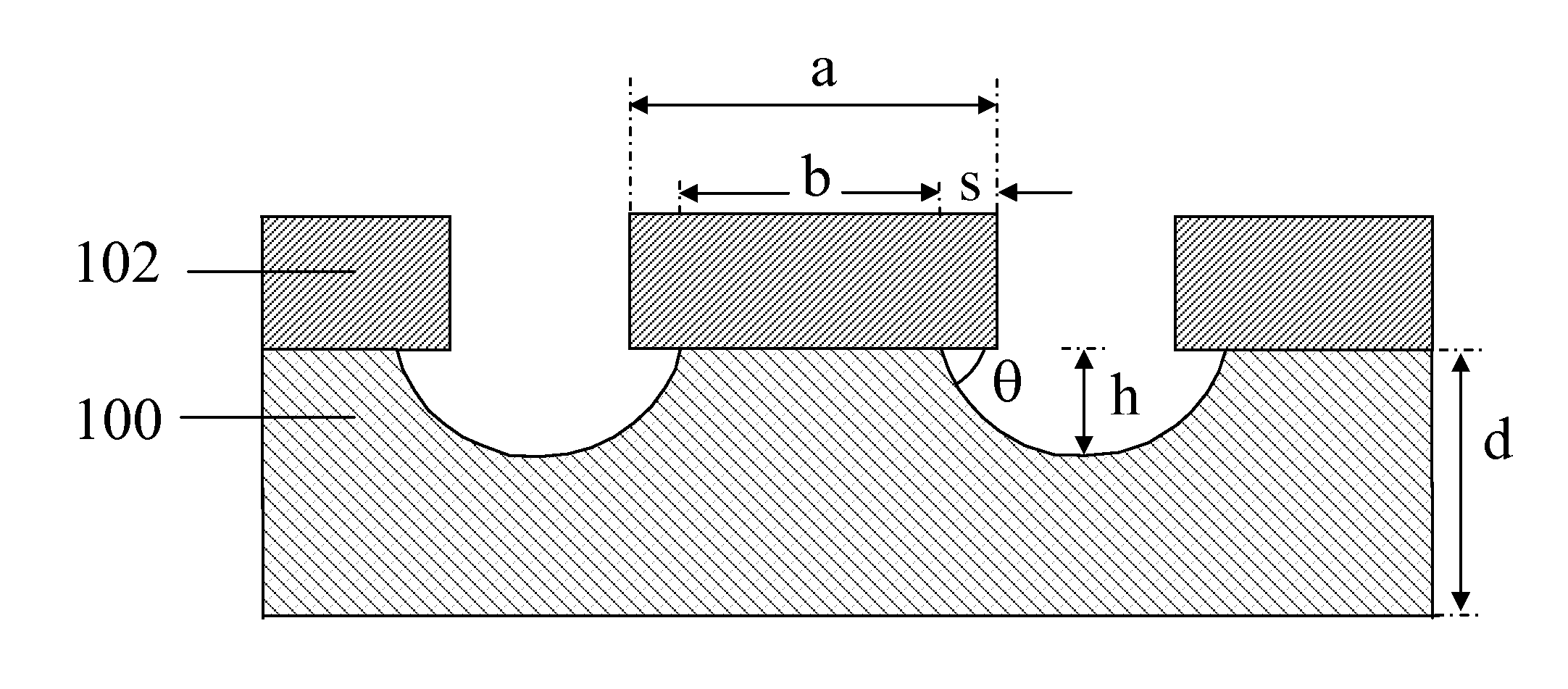
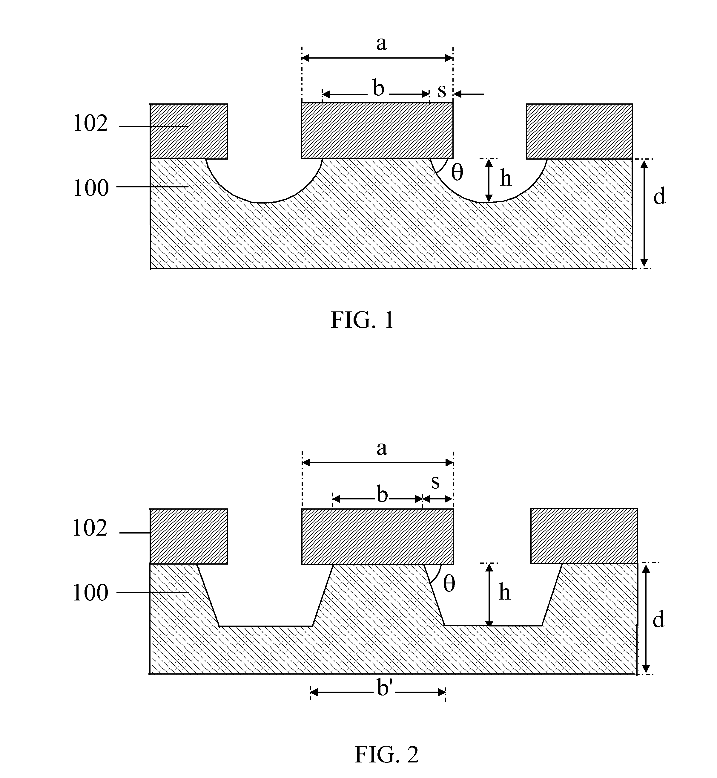
[0027]The present invention will enhance the reproducibility of the final product by displacing a difficult to control chemical etching process with a robust electrochemical machining process. Chemical etching is driven solely by the chemical reaction between the substrate and etching bath. Electrolytic etching is an etching process driven by an external power source that is controlled by the user. The present invention takes conventional electrolytic etching a step further through the sophisticated application of pulsed electric fields. A key advantage of the present invention is the ability to enhance anisotropic dissolution behavior, thereby increasing the achievable aspect ratio.
[0028]There is need for a method that can etch features with minimal undercutting and without the use of caustic chemicals in the plating bath in the manufacture of devices having small features, such as stents, fuel nozzles, cooling channels, bipolar plates for fuel cells, and microchannels for sensors, microfluidic devices, chemical reactors, and dialysis. More particularly, embodiments of the invention are useful in forming features that range in size from about 5 to about 1500 microns, e.g., microfluidic channels may range from about 5 to 300 microns, bipolar plates may range from about 500 to 1500 microns and cooling channels range from about 200 to 1500 microns.
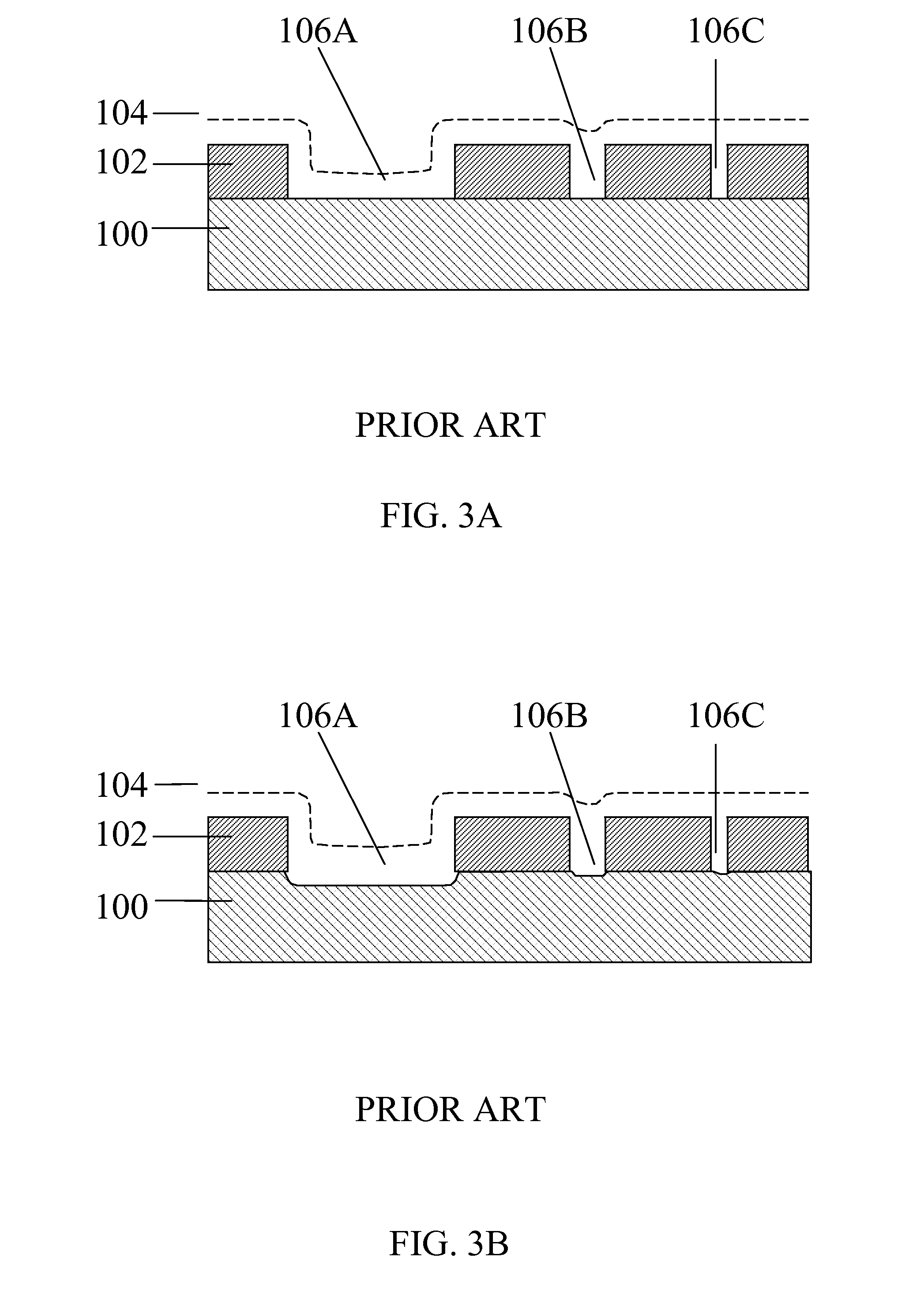
[0029]In one embodiment of the present invention, the exposed part of the metal layer, e.g. 440C stainless steel or copper, is electrochemically etched using an electric current in combination with a non-active electrolyte solution. As discussed herein, a “non-active” electrolyte solution is an electrolyte solution that does not provide chemical etching capability (e.g., the ability to electrolessly oxidize the metal forming the surface of the substrate) in the absence of an electric current. Further improvements on the disclosed electrochemical etching process are obtained using pulsed electric currents.

Problems solved by technology

As discussed herein, a “non-active” electrolyte solution is an electrolyte solution that does not provide chemical etching capability (e.g., the ability to electrolessly oxidize the metal forming the surface of the substrate) in the absence of an electric current.

Method used


Image

  • Electrochemical etching and polishing of conductive substrates
  • Electrochemical etching and polishing of conductive substrates
  • Electrochemical etching and polishing of conductive substrates

Examples


Embodiment Construction

[0048]The present invention provides a method for etching an exposed part of a metal substrate, specifically for the manufacture of devices having small features, such as fuel nozzles and stents and in the machining of cooling channels for thermal management in aerospace electronics. The method of the invention can be carried out using any suitable electrolytic etching apparatus. That apparatus includes a vessel which houses a counter electrode, which can be formed from any suitable electrode material such as titanium or platinum. In practice, the number of counter electrodes will be selected to facilitate achieving a uniform etching. The work piece to be treated is clamped in the vessel using a chuck in a position in which it is located opposite the counter electrode or counter electrodes. A power supply or rectifier completes a circuit whereby a net anodic electric current is delivered to the work piece, causing electrochemical etching of the exposed part of the metal layer, and a...


PUM

PropertyMeasurementUnit
Timeaaaaaaaaaa
Timeaaaaaaaaaa
Timeaaaaaaaaaa

Abstract

A method for electrochemically etching a metal layer through an etch-resist layer pattern using a non-active electrolyte solution is described. The method is particularly useful in fabrication of advanced fuel delivery systems for land-based power generation turbines and aerospace turbine engines; of components for advanced thermal management in aerospace electronic devices and in cooling channels; of stents used in medicine; and of microchannels for sensors, chemical reactors, and dialysis and the like. In one embodiment of the invention the metal layer is copper and the non-active electrolyte solution is a mixture of sodium nitrate and sodium chloride and a pulse electric current is employed to accomplish the electrochemical etching.

Description

CROSS REFERENCE TO RELATED APPLICATION[0001]This application claims the benefit of U.S. Provisional Application Ser. No. 61 / 228,660 filed Jul. 27, 2009, the entire contents of which are hereby incorporated by reference.STATEMENT REGARDING FEDERALLY SPONSORED RESEARCH OR DEVELOPMENT[0002]This invention was made with U.S. Government support under U.S. Department of Energy DE-FG02-08ER85112. The U.S. Government has certain rights in the invention.FIELD OF THE INVENTION[0003]The present invention relates to the fabrication of parts and devices by a photoelectrolytic machining or an electrolytic through mask etching method.[0004]One aspect of the present disclosure relates to the fabrication of fuel nozzles.[0005]Another aspect relates to the formation of cooling channels for thermal management for aerospace components.[0006]Another aspect relates to the manufacture of stents.[0007]Another aspect relates to the formation of microchannel reactors.[0008]Another aspect relates to the machin...

Claims


Application Information

Patent Timeline
IPC IPC(8): C25F3/02
CPCC25F7/00C25F3/14
Inventor TAYLOR, E. JENNINGSSUN, JENNY J.LOZANO-MORALES, ALONSOMCCRABB, HEATHERINMAN, MARIA E.
Owner FARADAY TECH INC
Learn More