
Semiconductor process

Active Publication Date: 2011-01-20
UNITED MICROELECTRONICS CORP
View PDF9 Cites 6 Cited by
  • Summary
  • Abstract
  • Description
  • Claims
  • Application Information

AI Technical Summary

Benefits of technology

[0008]Accordingly, the present invention provides a semiconductor process in which the possibility of generating a leakage path is reduced and the performance of the device is enhanced.
[0018]In the present invention, an annealing process is performed with high concentration of hydrogen before or after the step of etching the metal layer. Hydrogen can repair (or stabilize) the dangling bonds in a high temperature environment, so that the charges accumulated on the substrate are reduced and the possibility of leaking is reduced as well.

Problems solved by technology

However, plasma can move along the metal during the process and generates the so-called “antenna effect”, so that the device of the performance is affected.
If a leakage occurs in the capacitor, the data refresh frequency is increased, the data access speed is affected, and even an error in data access is caused.
The above-mentioned problems are generated in the process using plasma for fabricating the DRAM, such as a high density plasma chemical vapor deposition (HDPCVD) process for depositing a silicon oxide dielectric layer having a good filling property, or an etching process for etching aluminum with plasma.
That is, during the process using plasma, the charges accumulate on the surface of the dielectric layer, and move along the metal interconnection to the silicon substrate, so that a portion of the charges are captured by the dangling bonds of the silicon substrate to form a leakage path, resulting in serious problems such a short refresh time of the capacitor or a large distribution of the threshold voltage.

Method used


Image

  • Semiconductor process
  • Semiconductor process
  • Semiconductor process

Examples


example

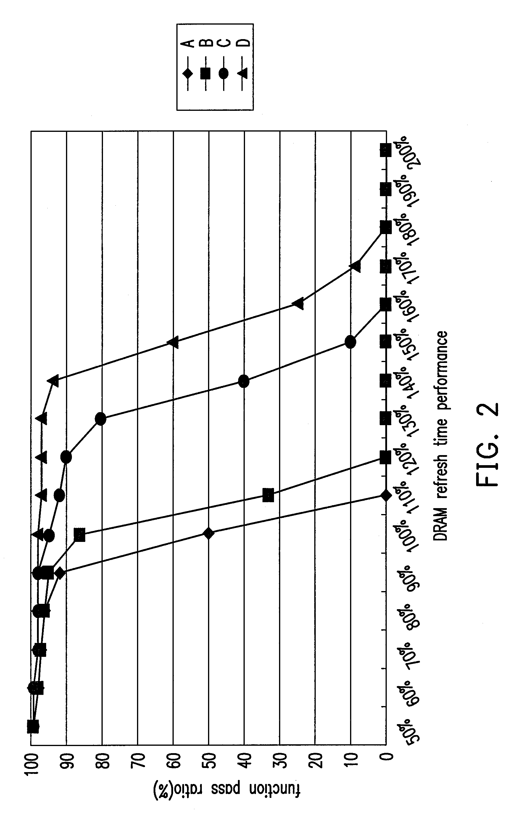
[0033]FIG. 2 schematically illustrates a diagram of function pass ratio as a function of DRAM fresh time performance under different annealing conditions according to an example of the present invention.

[0034]Referring to FIG. 2, line A represents the condition in which an annealing process is performed with hydrogen in a concentration of 71% after the step of etching the upmost aluminum layer to form the pad in the aluminum backend process. Line B represents the condition in which an annealing process is performed with hydrogen in a concentration of 9.1% after the step of etching the upmost aluminum layer to form the pad in the copper backend process. Line C represents the condition in which an annealing process is performed with hydrogen in a concentration of 71% before the step of etching the upmost aluminum layer to form the pad in the copper backend process. Line D represents the condition that an annealing process is performed with hydrogen in a concentration of 71% after the ...


PUM


Abstract

A semiconductor process is provided. First, a substrate having a dielectric layer formed thereon is provided. Thereafter, an interconnection structure including copper is formed in the dielectric layer. Afterwards, a metal layer is formed on the dielectric layer. The metal layer is then patterned to form a pad. An annealing process is performed, wherein the gas source for the annealing process includes hydrogen in a concentration of 50% to 90%.

Description

BACKGROUND OF THE INVENTION[0001]1. Field of Invention[0002]The present invention relates to a semiconductor process, and more particularly to a method for reducing a leakage path.[0003]2. Description of Related Art[0004]Plasma is a partially ionized gas, and is widely applied in a semiconductor process such as film deposition, etching or ion implantation. However, plasma can move along the metal during the process and generates the so-called “antenna effect”, so that the device of the performance is affected.[0005]For example, a dynamic random access memory (DRAM) cell stores data with a capacitor. The data of the memory cell is determined by the charges of the capacitor. The level of integration of memory cells is getting increased as the technology is getting developed. Meanwhile, the capacitance of the capacitor has to be increased as the dimension of the memory cell is getter smaller, so that the possibility of misjudging data is reduced, the data refresh frequency is reduced, ...

Claims


Application Information

Patent Timeline
IPC IPC(8): H01L21/768
CPCH01L21/32136H01L27/10897H01L23/53228H01L21/76838H01L2924/0002H10B12/50H01L2924/00
Inventor CHUN-CHILEH, FANGPO-JONG, CHENTSUNG-MIN, KUO
Owner UNITED MICROELECTRONICS CORP
Learn More