
Semiconductor laser apparatus, method of manufacturing the same and optical apparatus

a semiconductor laser and optical technology, applied in semiconductor lasers, instruments, record information storage, etc., can solve the problem of unlikely bonding of the second semiconductor laser device, and achieve the effect of improving the reliability of the aforementioned semiconductor laser apparatus, excellent yield and easy downsizing

Inactive Publication Date: 2011-01-13
SANYO ELECTRIC CO LTD
View PDF0 Cites 6 Cited by
  • Summary
  • Abstract
  • Description
  • Claims
  • Application Information

AI Technical Summary

Benefits of technology

The present invention is related to a semiconductor laser apparatus that includes two semiconductor laser devices bonded onto a support member. The first semiconductor laser device is bonded onto the support member through a first bonding layer, while the second semiconductor laser device is bonded onto the first semiconductor laser device through a second bonding layer. The second bonding layer has a lower melting point than the first bonding layer, and the second semiconductor laser device is positioned closer to the support member than the first semiconductor laser device. This allows for easy bonding of the second semiconductor laser device without damaging the first semiconductor laser device. The first and second semiconductor laser devices can be arranged close to each other, making it easy to downsize optical components and align the optical apparatus. The semiconductor laser apparatus is easy to mount on the optical apparatus and has improved temperature characteristics and reliability. The thickness of the first and second semiconductor device layers is controlled to equalize the heights of the light-emitting points of the semiconductor laser devices. This allows for precise control of the position of the light-emitting points when the semiconductor laser apparatus is used as a light source.

Problems solved by technology

Thus, the first semiconductor laser device can be inhibited from being damaged and the second semiconductor laser device can be excellently bonded onto the support member, and hence poor bonding of the second semiconductor laser device is unlikely to occur.

Method used


Image

  • Semiconductor laser apparatus, method of manufacturing the same and optical apparatus
  • Semiconductor laser apparatus, method of manufacturing the same and optical apparatus
  • Semiconductor laser apparatus, method of manufacturing the same and optical apparatus

Examples


first embodiment

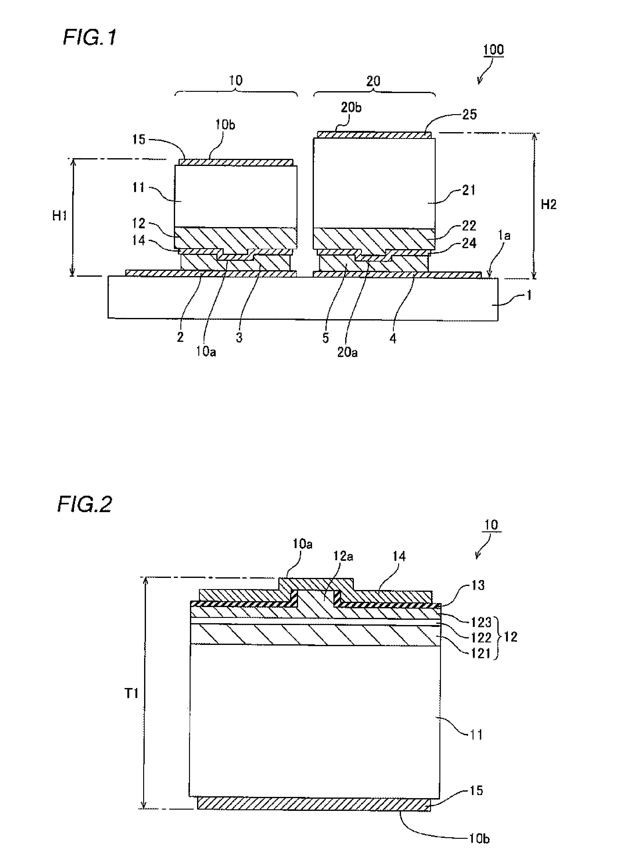
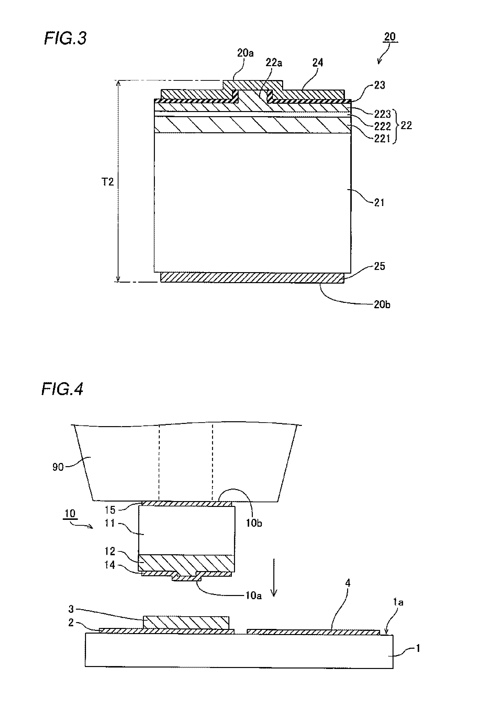
[0054]A structure of a semiconductor laser apparatus 100 according to a first embodiment of the present invention is now described with reference to FIGS. 1 to 3.

[0055]In the semiconductor laser apparatus 100, a blue-violet semiconductor laser device 10 and a red semiconductor laser device 20 are bonded onto an upper surface 1a of a submount 1 made of AlN to be adjacent to each other and are arranged such that laser beams thereof are emitted parallel to each other. The submount 1 and the upper surface 1a of the submount 1 are examples of the “support member” and the “main surface of the support member” in the present invention, respectively, and the blue-violet semiconductor laser device 10 and the red semiconductor laser device 20 are examples of the “first semiconductor laser device” and the “second semiconductor laser device” in the present invention, respectively. The submount 1 is also an example of the “heat radiation substrate” in the present invention.

[0056]The blue-violet s...

second embodiment

[0078]A case of forming a three-wavelength semiconductor laser apparatus by employing a red / infrared two-wavelength semiconductor laser device in place of the red semiconductor laser device in the aforementioned first embodiment is now described with reference to FIGS. 7 and 8. A structure similar to that in the aforementioned first embodiment is denoted by the same reference numerals and redundant description is omitted.

[0079]In a semiconductor laser apparatus 200 according to the second embodiment of the present invention, a blue-violet semiconductor laser device 10 and the red / infrared two-wavelength semiconductor laser device 30 are bonded to be adjacent to each other and are arranged such that laser beams thereof are emitted parallel to each other, as shown in FIG. 7. The red / infrared two-wavelength semiconductor laser device 30 is an example of the “second semiconductor laser device” in the present invention. The red / infrared two-wavelength semiconductor laser device 30 is bon...

third embodiment

[0102]An optical pickup 1000 according to a third embodiment of the present invention is now described with reference to FIGS. 12 to 14. The optical pickup 1000 is an example of the “optical apparatus” in the present invention.

[0103]As shown in FIG. 12, the optical pickup 1000 according to the third embodiment comprises a semiconductor laser apparatus 300 emitting laser beams of three wavelengths of blue-violet, red and infrared, an optical system 400 adjusting the laser beams emitted from the semiconductor laser apparatus 300 and a light detection portion 410 receiving the laser beams.

[0104]The semiconductor laser apparatus 300 has a base 301 made of a conductive material, a cap 302 arranged on a front surface of the base 301 and leads 303, 304, 305 and 306 mounted on a rear surface of the base 301, as shown in FIGS. 13 and 14. A header 301a is integrally formed with the base 301 on the front surface of the base 301. The aforementioned semiconductor laser apparatus 200 is arranged ...


PUM


Abstract

This semiconductor laser apparatus includes a support member having a main surface, a first semiconductor laser device bonded onto the main surface through a first bonding layer and a second semiconductor laser device bonded onto the main surface through a second bonding layer to be adjacent to the first semiconductor laser device. The melting point of the second bonding layer is lower than that of the first bonding layer, and a first height from the main surface to a fourth surface of the second semiconductor laser device is larger than a second height from the main surface to a second surface of the first semiconductor laser device.

Description

CROSS-REFERENCE TO RELATED APPLICATION[0001]The priority application number JP2009-162133, Semiconductor Laser Apparatus, Method of Manufacturing the Same, Optical Pickup and Optical Apparatus, Jul. 8, 2009, Yasuyuki Bessho et al, upon which this patent application is based is hereby incorporated by reference.BACKGROUND OF THE INVENTION[0002]1. Field of the Invention[0003]The present invention relates to a semiconductor laser apparatus, a method of manufacturing the same and an optical apparatus, and more particularly, it relates to a semiconductor laser apparatus loaded with a plurality of hybrid integrated semiconductor laser devices, a method of manufacturing the same and an optical apparatus employing the same.[0004]2. Description of the Background Art[0005]An optical pickup comprising a semiconductor laser apparatus, optical components such as a lens, a beam splitter (BS) etc., a photodetector and so on is employed in an optical disc device for at least either recording informa...

Claims


Application Information

Patent Timeline
Patent Type & Authority Applications(United States)
IPC IPC(8): H01S5/40H01S5/323H01L21/50
CPCB82Y20/00G11B7/1275H01S5/0207H01S5/02212H01S5/0224H01S5/02272H01L2224/83192H01S5/34326H01S5/34333H01S5/4031H01S5/4087H01L2224/83191H01S5/22H01S5/0234H01S5/0237
Inventor BESSHO, YASUYUKIGONSUI, KOJISHIMIZU, GENMIHASHI, DAIKIOOTA, KIYOSHI
Owner SANYO ELECTRIC CO LTD
Learn More