Methods for fabricating copper indium gallium diselenide (CIGS) compound thin films
a technology of copper indium gallium diselenide and compound thin film, which is applied in the direction of coating, semiconductor devices, chemical vapor deposition coating, etc., can solve the problems of uneven film roughness, large manufacturing and high power consumption, and large manufacturing and fabrication costs for silicon solar cells
- Summary
- Abstract
- Description
- Claims
- Application Information
AI Technical Summary
Problems solved by technology
Method used
Image


Examples
example 1
[0037]A glass substrate was cleaned by immersion into a glass detergent and an ultrasonic vibrator was used to enhance glass cleaning performance. The cleaned glass substrate was then immersed in (deionized water) DI water and rinsed with DI water until no glass detergent was left. Next, the glass substrate was placed into an oven at a temperature of 150° C. to dry out the glass substrate. The cleaned glass substrate was instantly placed into a sputtering tool vacuum chamber and a pressure in the vacuum chamber was reduced to below 1*10−6 torr by a vacuum pump. When the pressure in the vacuum chamber achieved a high pressure, an argon flow was transported to the vacuum chamber at a flow rate of 10 sccm to recover the pressure in the vacuum chamber to 10 mtorr. At this time, a DC sputtering process was performed under the pressure of 10 mtorr to form a first Mo thin film with a thickness of about 400 nm. The first Mo thin film had good adhesion to the glass substrate, thereby serving...
example 2
[0039]A glass substrate was cleaned by immersion into a glass detergent and an ultrasonic vibrator was used to enhance glass cleaning performance. The cleaned glass substrate was then immersed in (deionized water) DI water and rinsed with DI water until no glass detergent was left. Next, the glass substrate was placed into an oven at a temperature of 150° C. to dry out the glass substrate. The cleaned glass substrate was instantly placed into a sputtering tool vacuum chamber and a pressure in the vacuum chamber was reduced to below 1*10−6 torr by a vacuum pump. When the pressure in the vacuum chamber achieved a high pressure, an argon flow was transported to the vacuum chamber at a flow rate of 10 sccm to recover the pressure in the vacuum chamber to 2 mtorr. At this time, a DC sputtering process was performed under the pressure of 10 mtorr to form a titanium (Ti) thin film with a thickness of about 100 nm. The Ti thin film showed good adhesion to the glass substrate, thereby servin...
example 3
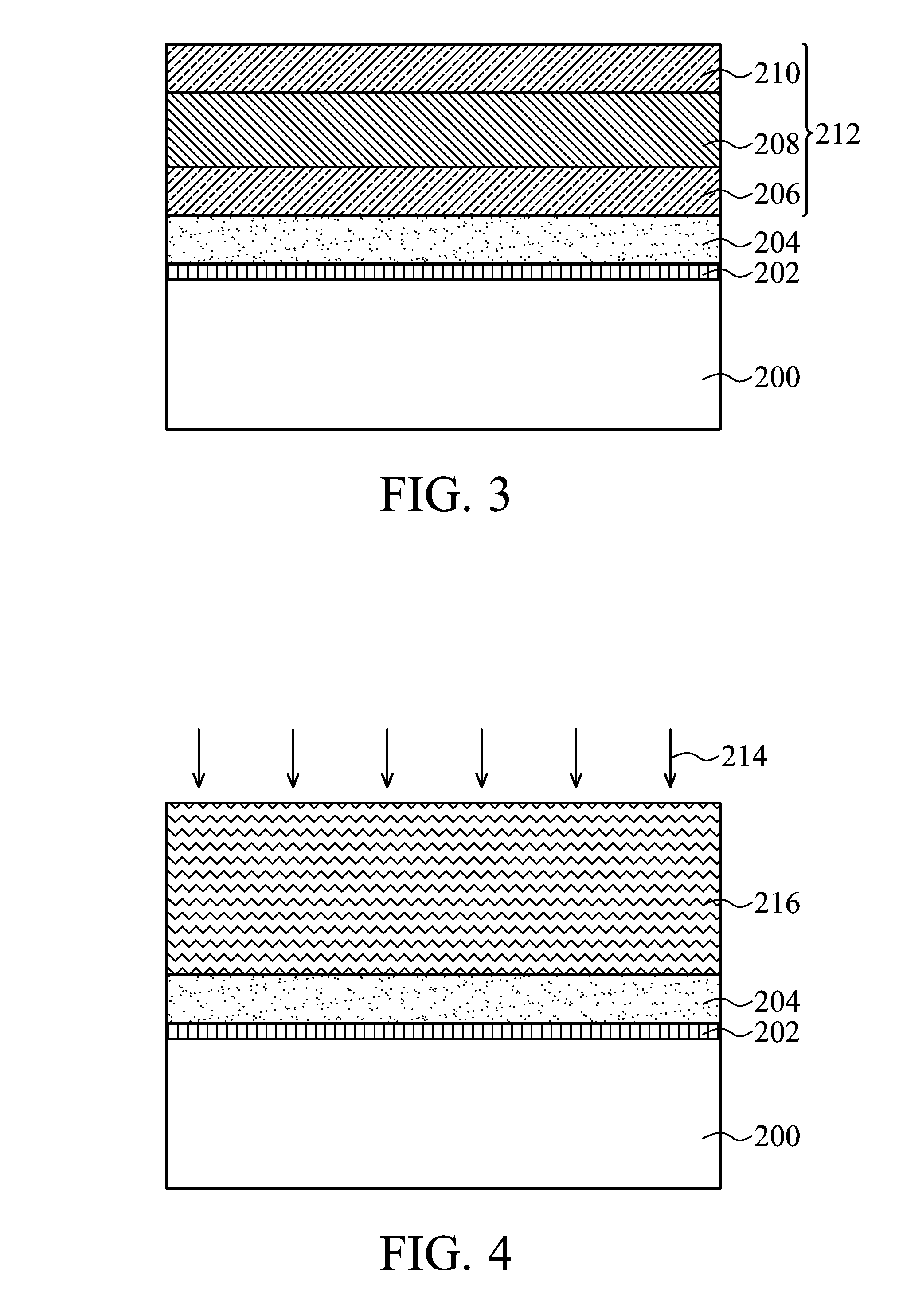
[0040]A glass substrate with an adhesive layer formed thereon was provided. An Mo thin film was formed over the adhesive layer by sputtering method. The Mo thin film was formed with a thickness of about 600 nm and the adhesive layer was the first Mo thin film used in Example 1, or a metal thin film made of Ti, Ta, Cr, Co, Ni, W, or combinations thereof. Next, a stacked film comprising Cu0.73Ga0.27 / Cu0.48In0.52 / Cu0.73Ga0.27 composite structure shown in FIG. 3 was formed over the Mo thin film by a DC sputtering process. Alloy targets of Cu0.73Ga0.27 and Cu0.48In0.52 were used as precursor materials, and a Cu0.73Ga0.27 alloy thin film with a thickness of 100 nm was sputtered over the composite structure comprising the Mo thin film and the glass substrate at a power of 160 W, and a Cu0.48Ga0.52 alloy thin film with a thickness of 600 nm was then sputtered over the Cu0.73Ga0.27 alloy thin film under a reduced power of 60 W. Next, another Cu0.73Ga0.27 alloy thin film with a thickness of 2...
PUM
| Property | Measurement | Unit |
|---|---|---|
| thickness | aaaaa | aaaaa |
| thickness | aaaaa | aaaaa |
| temperature | aaaaa | aaaaa |
Abstract
Description
Claims
Application Information
 - Generate Ideas
- Intellectual Property
- Life Sciences
- Materials
- Tech Scout
- Unparalleled Data Quality
- Higher Quality Content
- 60% Fewer Hallucinations
Browse by: Latest US Patents, China's latest patents, Technical Efficacy Thesaurus, Application Domain, Technology Topic, Popular Technical Reports.
© 2025 PatSnap. All rights reserved.Legal|Privacy policy|Modern Slavery Act Transparency Statement|Sitemap|About US| Contact US: help@patsnap.com