Method of manufacturing light - absorbtion layer of solar cell through selenization process under elemental selenium vapor atmosphere and thermal processing apparatus for manufacturing light - absorbing layer

a technology of selenium vapor atmosphere and light absorbing layer, which is applied in the manufacture of final products, basic electric elements, coatings, etc., can solve the problems of low material utilization and high cost apparatus, difficulty in large-area deposition, and low throughput, and achieves high efficiency and reduces the production cost of the cigs light absorbing layer. , the effect of high efficiency

Inactive Publication Date: 2014-03-13
SOLARDIN INC
View PDF3 Cites 152 Cited by
  • Summary
  • Abstract
  • Description
  • Claims
  • Application Information

AI Technical Summary

Benefits of technology

[0018]According to the present invention, it is possible to provide a high efficiency CIGS method of manufacturing a light absorbing layer through a method where CIG/CI thin films are formed on an electrode and, after that, thermal treatment is performed under an element selenium vapor ambience and to prov

Problems solved by technology

Although high efficiency of 20% is obtained in the laboratory, the aforementioned co-evaporation method has problems of low material utilization and high cost apparatuses, difficulties in large-area deposition, relatively low throughput, and the like, which are to overcome for commercialization thereof.
However, in order to solve problems of surface tension due to viscosity of liquefied selenium, non-uniform evaporation due to inevitable non-uniformity of temperature, damage to molybdenum electrode due to diffusion of liquefied selenium into a molybdenum electrode, and the like, a temperature of a thermal treatment process, evaporation flux, and other complex factors needs to be very accurately controlled.
Thus, the above-mentioned methods have technical difficulty in commercialization.
However, the method has problems of high cost and toxicity of reaction gases to be solved.
As one of selenizati

Method used


Image

  • Method of manufacturing light - absorbtion layer of solar cell through selenization process under elemental selenium vapor atmosphere and thermal processing apparatus for manufacturing light - absorbing layer
  • Method of manufacturing light - absorbtion layer of solar cell through selenization process under elemental selenium vapor atmosphere and thermal processing apparatus for manufacturing light - absorbing layer
  • Method of manufacturing light - absorbtion layer of solar cell through selenization process under elemental selenium vapor atmosphere and thermal processing apparatus for manufacturing light - absorbing layer

Examples


first embodiment

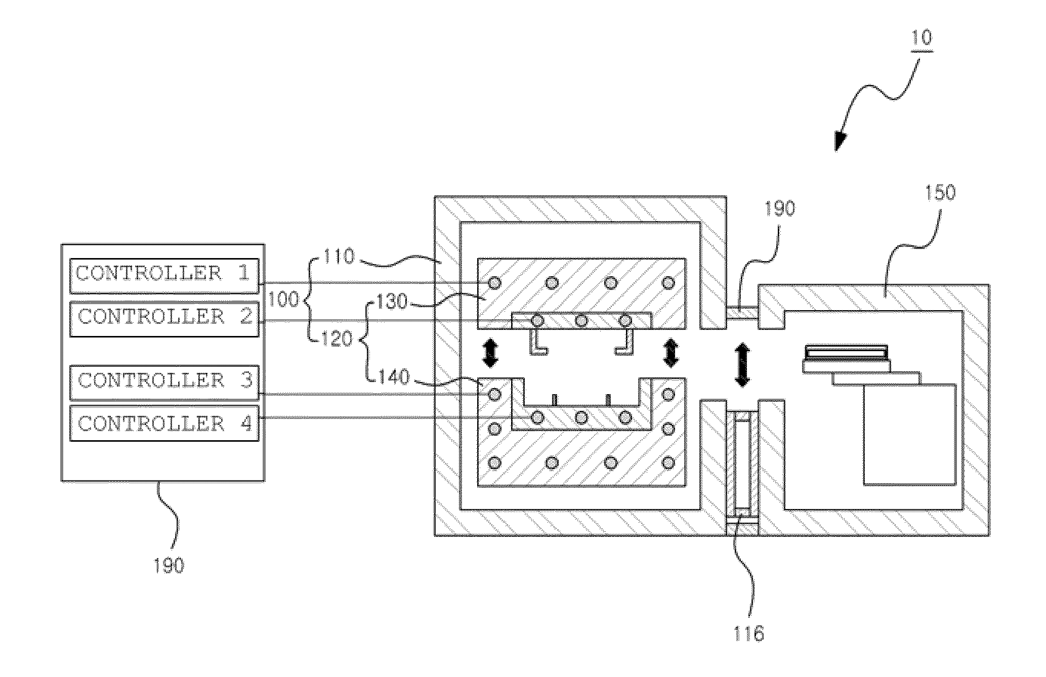
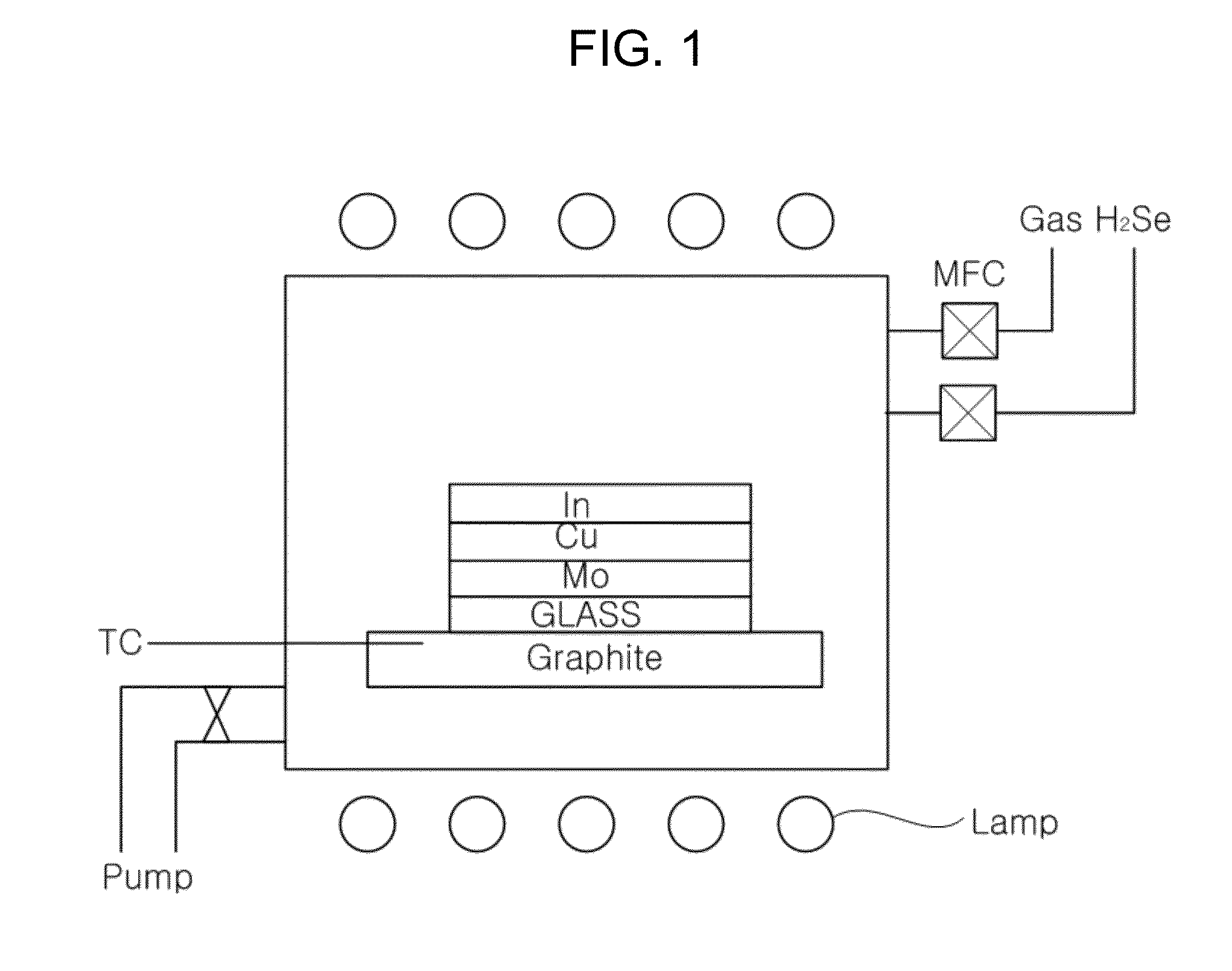
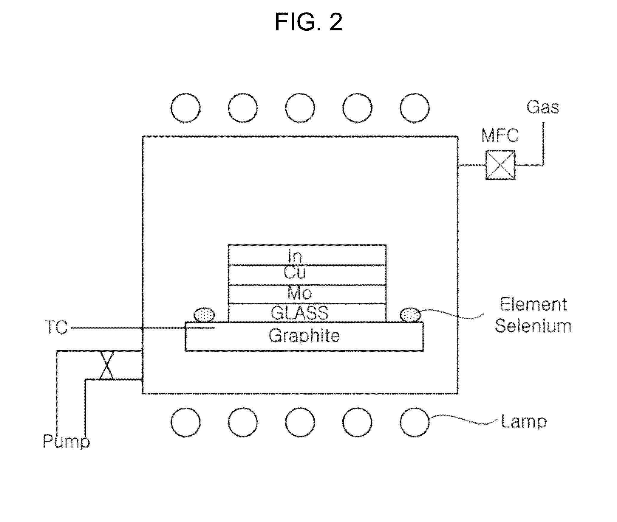
[0050]FIG. 3 is a flowchart illustrating a sequence of processes of a method of manufacturing a light absorbing layer according to a first embodiment of the present invention. Referring to FIG. 3, the method is configured to include a step (Step 300) of controlling the temperature of all the wall of a sealed chamber to be a predefined thin film formation temperature, a step (Step 310) of loading a specimen where copper, indium, and gallium are laminated and selenium on a susceptor and inserting the susceptor into a chamber, and a step (S320) of heating the specimen by driving a heat source disposed under the susceptor and simultaneously heating element selenium by driving a heat source disposed above the susceptor. In Step 320, in order to allow the selenium not to be condensed on the specimen during the heating process, the temperature of the element selenium is controlled by using the heat source disposed above the susceptor so that the selenium vapor pressure in the vicinity of t...

second embodiment

[0083]Hereinafter, a sequence of processes of a method of forming the CIGS thin film on the substrate by using the manufacturing method according to the present invention will be described. The method of manufacturing the CIGS solar cell is configured to include a step of forming a back-side electrode layer on a soda lime glass (soda lime glass) substrate which is rinsed by RCA, a step of forming a light absorbing layer, a step of forming a buffer layer, a step of forming an I—ZnO layer, a step of forming a window layer, a step of forming an anti-reflection layer, and a step of forming a grid electrode layer and performing electrode wiring.

[0084]More specifically, in the method of manufacturing the CIGS solar cell, the substrate is formed with a thickness of 1 mm to 3 mm by using a soda lime glass. After the substrate is prepared, the substrate is rinsed through an RCA rinsing method by using deionized (DI) water. Besides the soda lime glass, a ceramic substrate such as alumina, a m...

third embodiment

[0090]In the method of the related art, there is a problem in that lower precipitation of gallium occurs during the selenization process, so that the efficiency is decreased. In order to solve the problem, one or two of sulfur(S) and a compound containing Na and the selenium are injected during the selenization process to sublimate Na functioning as a catalyst for forming high-quality CIGS, to prevent lower precipitation of gallium, and to improve the band gap. In this manner, during the selenization process, the selenium and one or two of sulfur(S) and a compound containing Na are injected, so that it is possible to generate a high-quality CIGS light absorbing layer.

[0091]While the present invention has been particularly shown and described with reference to exemplary embodiments thereof, it will be understood by those skilled in the art that various changes in form and details may be made therein without departing from the spirit and scope of the invention as defined by the append...


PUM

PropertyMeasurementUnit
Weightaaaaaaaaaa
Weightaaaaaaaaaa
Weightaaaaaaaaaa

Abstract

The method of manufacturing a light absorbing layer for a solar cell by performing thermal treatment on a specimen configured to include thin films of one or more of copper, indium, and gallium on a substrate and element selenium, includes steps of: (a) heating a wall of a chamber up to a predefined thin film formation temperature in order to maintain a selenium vapor pressure; (b) mounting the specimen and the element selenium on the susceptor at the room temperature and loading the susceptor in the chamber; and (c) heating the specimen in the lower portion of the susceptor and, at the same time, heating the element selenium in the upper portion of the susceptor, wherein, in the step (c), in order for liquefied selenium not to be condensed on the specimen which is loaded at the room temperature and is not yet heated, the temperature of the element selenium and the specimen loaded in the chamber are individually controlled, so that the selenium vapor pressure of an inner space of the chamber does not exceed a saturation vapor pressure corresponding to the temperature of the specimen.

Description

TECHNICAL FIELD[0001]The present invention relates to a method of manufacturing a light absorbing layer for a solar cell and a thermal treatment apparatus for manufacturing a light absorbing layer for a solar cell, and more particularly, a method of manufacturing a light absorbing layer for a solar cell using a selenization process capable of manufacturing a high-efficiency, large-area CIGS light absorbing layer in a short time by performing thermal treatment under an element selenium vapor ambience and a thermal treatment apparatus for manufacturing a light absorbing layer for a solar cell, which is suitable for implementing the method.BACKGROUND ART[0002]At recent, a ternary thin film such as CuInSe2 (hereinafter, referred to as ‘CIS’) or CuIn1-xGaxSe2 (hereinafter, referred to as ‘CIGS’) as one of compound semiconductor has been actively researched. Unlike silicon solar cells in the related art, the CIS-based thin film solar cells can be manufactured with a thickness of 10 micron...

Claims


Application Information

Patent Timeline
IPC IPC(8): H01L31/18
CPCH01L31/1876H01L21/02568H01L21/02579H01L21/02614H01L31/0322Y02E10/541Y02P70/50H01L31/04H01L31/18
Inventor SONG, SEONG HOON
Owner SOLARDIN INC
Why Eureka
Try Eureka