Magnetic Tunnel Junction Device and Fabrication

a technology of magnetic tunnel junction and device, which is applied in the direction of solid-state devices, semiconductor devices, instruments, etc., can solve the problems of reducing the tunneling magnetoresistance (tmr) of the mtj elements, affecting the integration of both types of processes together, and adding to the surface roughness in the mram areas. , to achieve the effect of avoiding the formation of recesses, avoiding surface roughness concerns, and avoiding the damage of logic layers

Inactive Publication Date: 2010-11-18
QUALCOMM INC
View PDF15 Cites 81 Cited by
  • Summary
  • Abstract
  • Description
  • Claims
  • Application Information

AI Technical Summary

Benefits of technology

[0004]The MRAM and logic processes may be integrated together, eliminating the surface roughness concerns for the MTJ devices and avoiding formation of recesses in the interlayer dielectric (ILD) portions of the logic areas. Damage to logic layers in the logic areas due to MRAM processing may be avoided by implementing a bottom cap layer formed before a copper damascene process is performed. The copper surface roughness impact may be avoided by moving the MTJ device away from the copper pad. The added series resistance of a bottom via may be avoided by directly contacting a bottom electrode of the MTJ to the copper pad. Surface roughness of the bottom cap layer may be reduced by first depositing the bottom electrode on the bottom cap layer and then adding MTJ films on the bottom electrode. The MRAM processes may be performed before the logic processes are performed. A top via may be added to selectively open the top of the MTJ device. The height of the top via may be adjustable.

Problems solved by technology

It may be challenging to integrate both types of processes together without negatively impacting both the MRAM areas and the logic areas.
Similarly, certain logic processes, if performed earlier in the sequence of process steps, may add to surface roughness in the MRAM areas.
In addition, bottom vias used with conventional MTJ elements may add series resistance to the MTJ elements, which may degrade a tunneling magnetoresistance (TMR) of the MTJ elements.

Method used


Image

  • Magnetic Tunnel Junction Device and Fabrication
  • Magnetic Tunnel Junction Device and Fabrication
  • Magnetic Tunnel Junction Device and Fabrication

Examples


Embodiment Construction

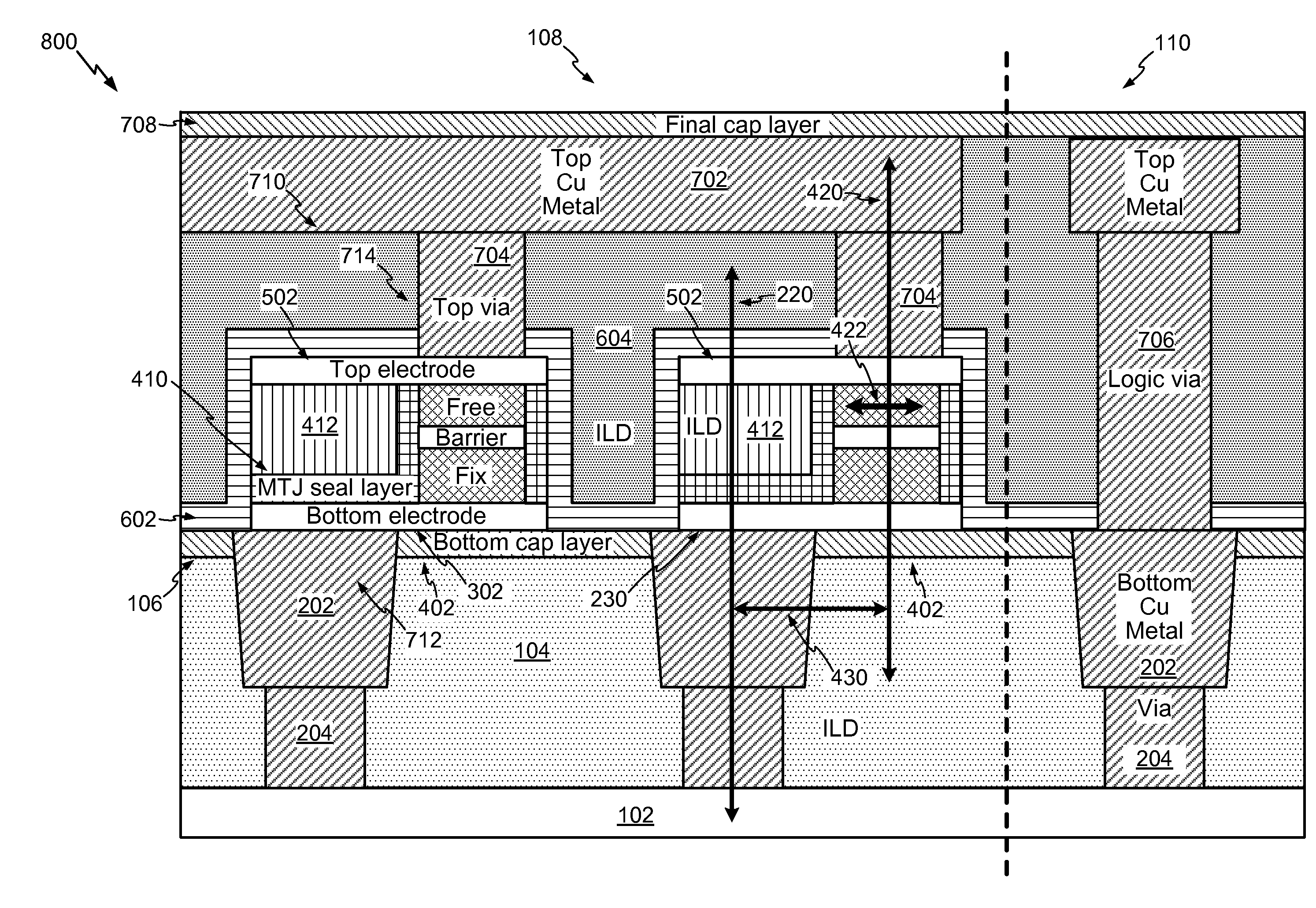
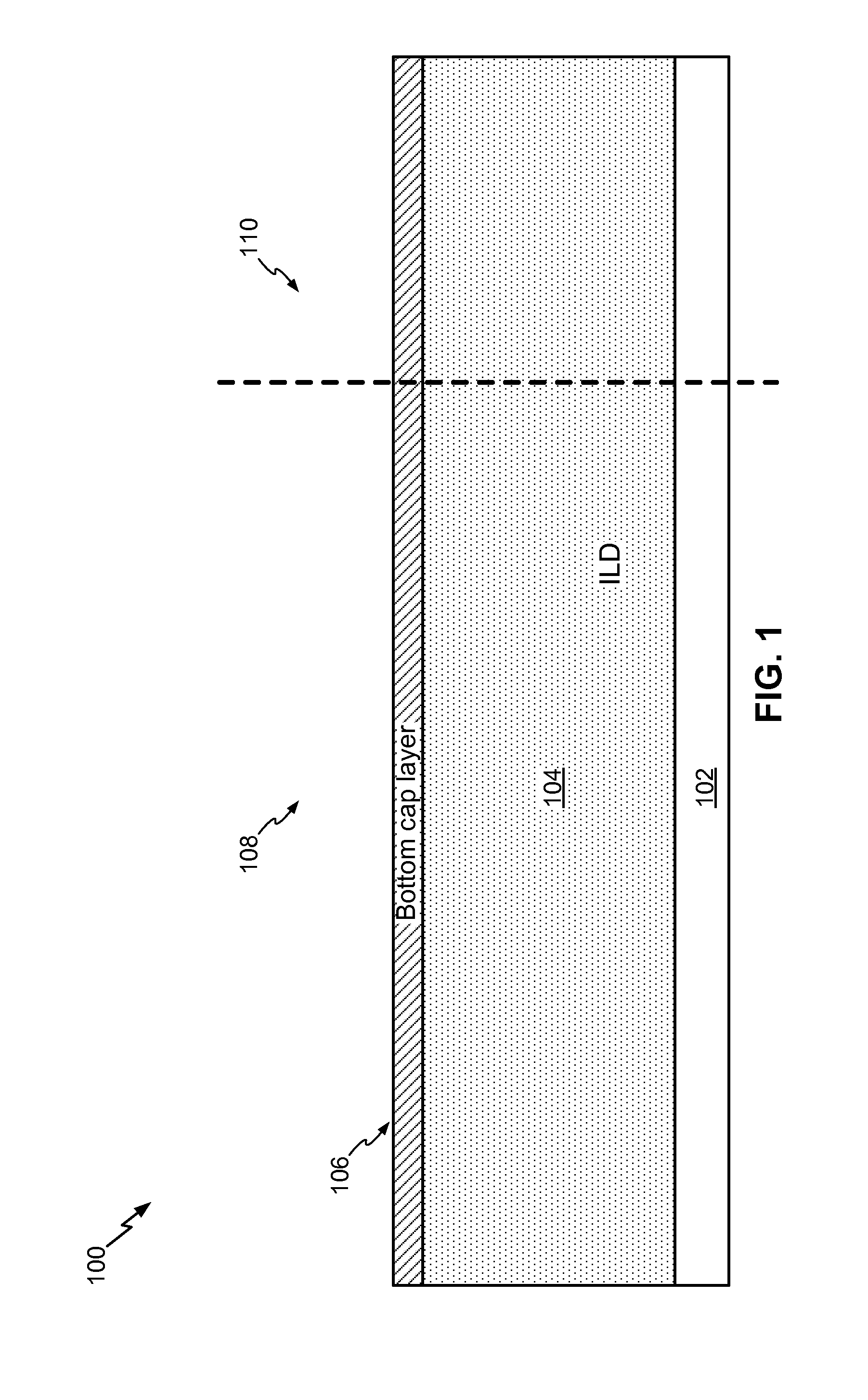
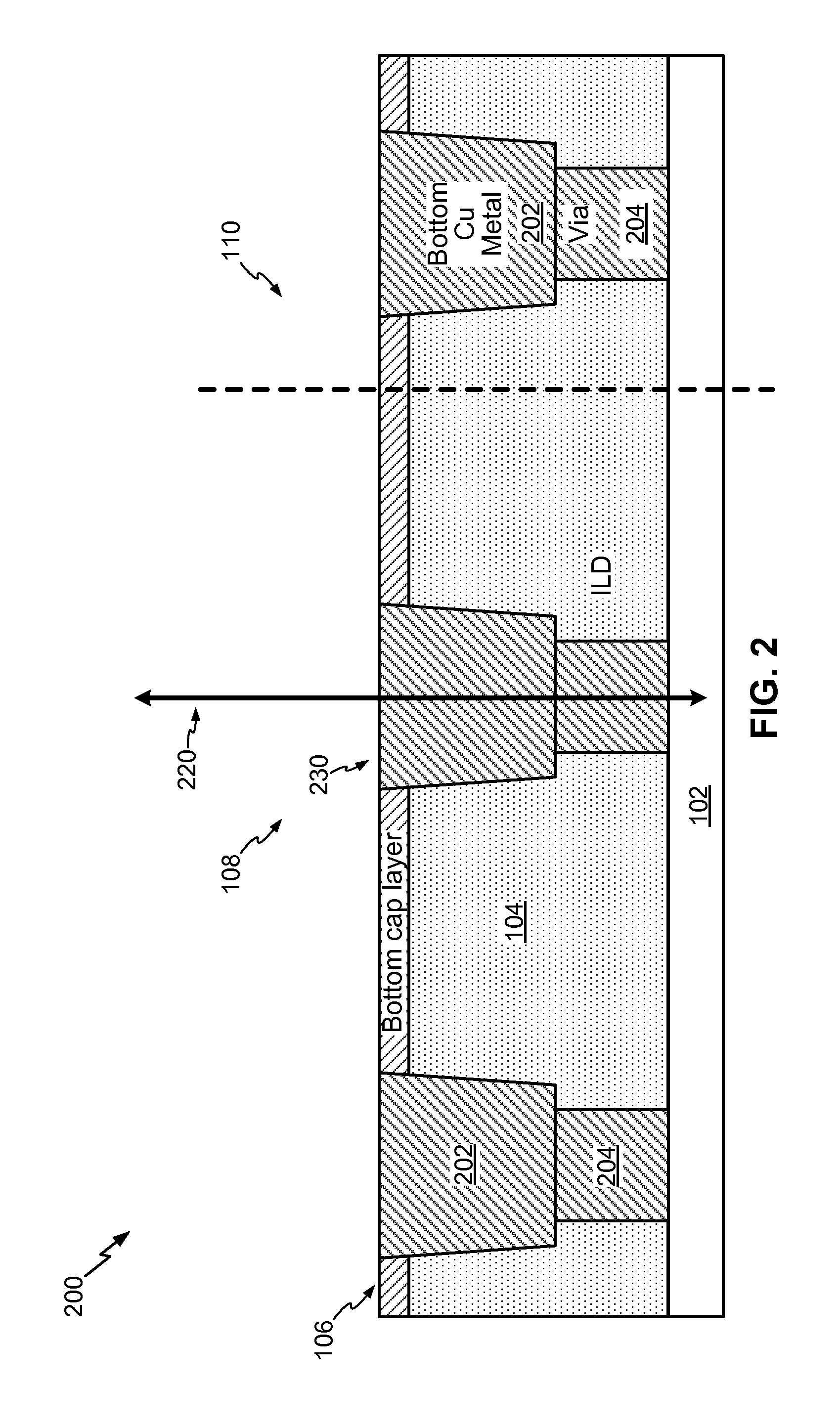
[0022]Particular embodiments of the present disclosure are described below with reference to the drawings. In the description, common features are designated by common reference numbers through the drawings. Referring to FIG. 1, a first illustrative diagram of at least one stage in the process of fabricating a magnetic tunnel junction (MTJ) device is depicted and generally designated 100. A first insulating layer 104 may be formed above a substrate 102. The substrate 102 represents any underlying layer, such as a cap layer for other underlying layers. For example, the first insulating layer 104 may be formed of material that is deposited on the substrate 102. A bottom cap layer 106 may be formed above the first insulating layer 104. For example, the bottom cap layer 106 may be formed of material that is deposited on the first insulating layer 104. In a particular embodiment, the bottom cap layer 106 includes silicon carbide (SiC) or silicon nitride (SiN, etc.). An MRAM area 108 of a...


PUM


Abstract

A magnetic tunnel junction (MTJ) device and fabrication method is disclosed. In a particular embodiment, a method is disclosed that includes forming a magnetic tunnel junction (MTJ) device on a structure that includes a bottom cap layer and a bottom metal-filled trench having a normal axis, the magnetic tunnel junction device including a bottom electrode, magnetic tunnel junction layers, a magnetic tunnel junction seal layer, a top electrode, and a logic cap layer, the magnetic tunnel junction device having an MTJ axis that is offset from the normal axis.

Description

I. FIELD[0001]The present disclosure is generally related to magnetic tunnel junction (MTJ) devices and fabrication.II. DESCRIPTION OF RELATED ART[0002]MTJ elements may be used to create a magnetic random access memory (MRAM). An MTJ element typically includes a pinned layer, a magnetic tunnel barrier, and a free layer, where a bit value is represented by a magnetic moment in the free layer. A bit value stored by an MTJ element is determined by a direction of the magnetic moment of the free layer relative to a direction of a fixed magnetic moment carried by the pinned layer. The magnetization of the pinned layer is fixed while the magnetization of the free layer may be switched.[0003]MRAM areas containing MTJ elements and logic areas containing logic and control elements may be fabricated on the same wafer. The structures and process sequences used to form the MTJ elements are generally different from the structures and process sequences used to form the logic and control elements. ...

Claims


Application Information

Patent Timeline
Patent Type & Authority Applications(United States)
IPC IPC(8): H01L29/82H01L43/12G06F19/00
CPCG11C11/16H01L27/222H01L43/02G11C11/15H01L43/12G11C11/161H10B61/00H10N50/80H10N50/01H10N50/10H10N59/00
Inventor LI, XIAKANG, SEUNG H.ZHU, XIAOCHUN
Owner QUALCOMM INC
Why Eureka
Try Eureka