Printed Wiring Board

Active Publication Date: 2010-09-16
NIPPON MEKTRON LTD
View PDF7 Cites 7 Cited by
  • Summary
  • Abstract
  • Description
  • Claims
  • Application Information

AI Technical Summary

Benefits of technology

[0028]Also, as the wiring pitch of the wire-type grounding conductors is 1 / n the signal line width (where n is a natural number of 1 or 2), overlapping areas of signal lines and grounding conductors located opposite to each other can be kept constant even in case of misalignment.
[0029]In so doing, by using a low dielectric constant material such as polyimide, liquid crystal polymer, or fluororesin as an interlayer insulating resin of a substrate, it is possible to reduce capacitance between the signal lines and grounding conductors.
[0030]This allows signal line width to be increased, making it possible to increase thickness of the wire-type grounding conductors laid out in parallel to the signal lines, and thus reduce difficulty of an etching process.
[0031]Also, the above-described materials, which normally have a lower dielectric-loss factor than a glass-epoxy board, can reduce dielectric losses at radio frequencies. Thus, these materials are advantageous for high-speed signal transmission.
[0033]This makes it possible to provide a printed wiring board which has a microstrip line structure suitable for high-speed signal transmission and thereby contribute to size reduction and performance improvement of electronic equipment.

Problems solved by technology

In this case, impedance mismatch has an impact when a 5-GHz or higher-frequency signal is transmitted.

Method used


Image

  • Printed Wiring Board
  • Printed Wiring Board
  • Printed Wiring Board

Examples


first embodiment

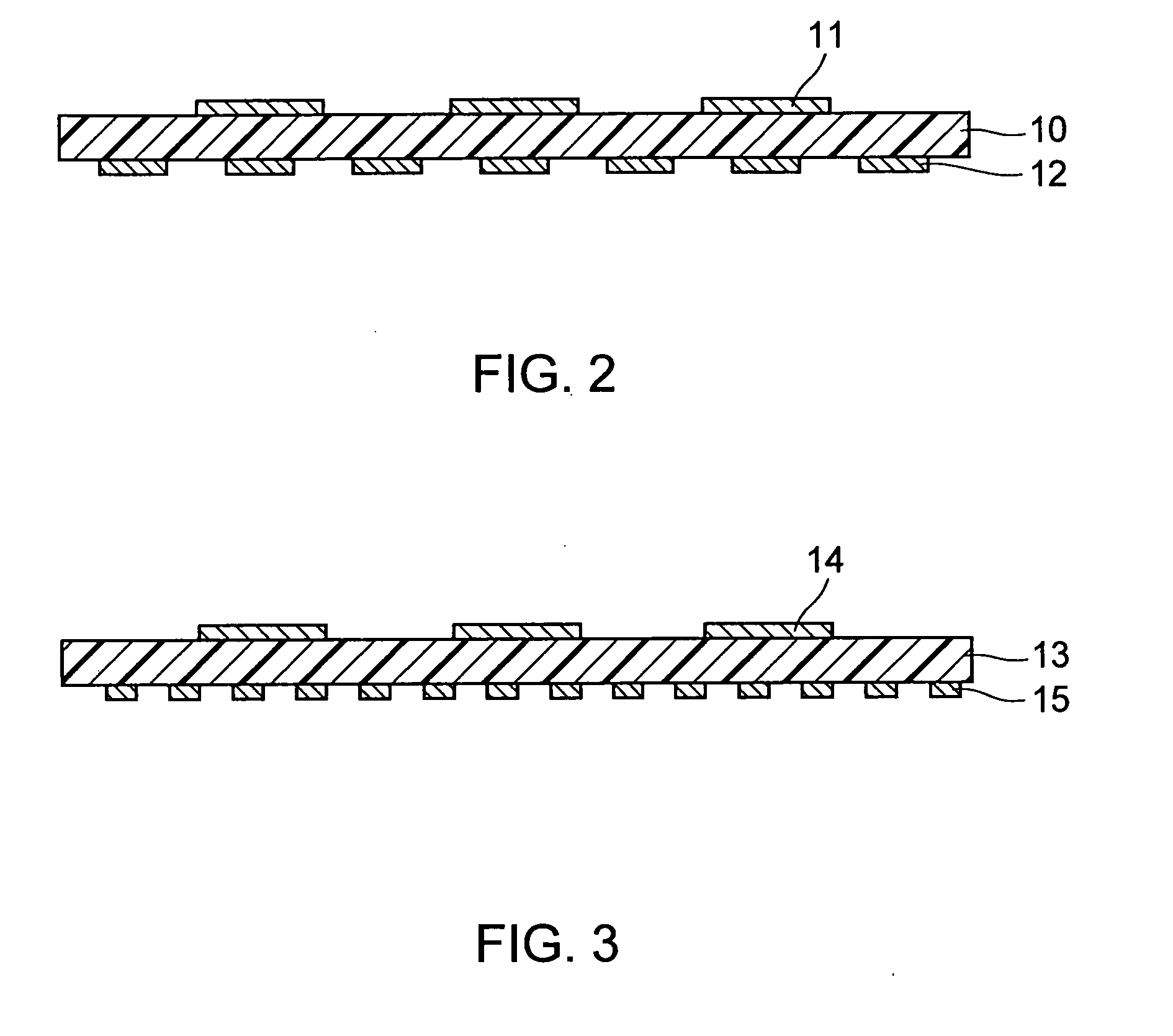
[0050]FIG. 2 is a sectional diagram of a microstrip line according to an embodiment of the present invention.

[0051]A double-sided copper-clad laminate named Metaloyal PI-25D-CCW-08D0 (#25) (manufactured by Toyo Metallizing Co., LTD.) is used as a starting material.

[0052]This material has been selected for the following two reasons.

[0053](1) In a microstrip line, a high dielectric factor of a substrate will increase capacitance between signal lines and grounding conductors, making it necessary to decrease signal line width to obtain desired characteristic impedance.

[0054]However, a narrow signal line width will increase the difficulty of forming wiring lines, making it impossible to accurately control impedance. Thus, polyimide which has a low dielectric factor is desirable for the substrate.

[0055](2) Copper foils used for copper-clad sheets normally go through a roughing process known as backside processing to ensure adherence to the substrate. However, increased inductance caused b...

second embodiment

[0058]FIG. 3 is a sectional view according to a second embodiment of the present invention. According to the second embodiment, a liquid crystal polymer is used for a substrate 13 instead of the polyimide according to the first embodiment, the liquid crystal polymer having a lower dielectric factor. This further reduces the capacitance between signal lines and grounding conductors, making it easier to process the signal lines of the given width.

[0059]Also, liquid crystal polymers, which have a lower dielectric-loss factor than polyimide, can reduce dielectric losses at radio frequencies. Thus, liquid crystal polymers are advantageous for high-speed signal transmission. A double-sided copper-clad laminate named ESPANEX LB-09-25-09NE (manufactured by Nippon Steel Chemicals Co., LTD.) is used as a starting material.

[0060]A substrate of a liquid crystal polymer is 25 μm thick and a copper foil which is originally 9 μm thick is half-etched to 5 μm. A microstrip line is formed using the h...

third embodiment

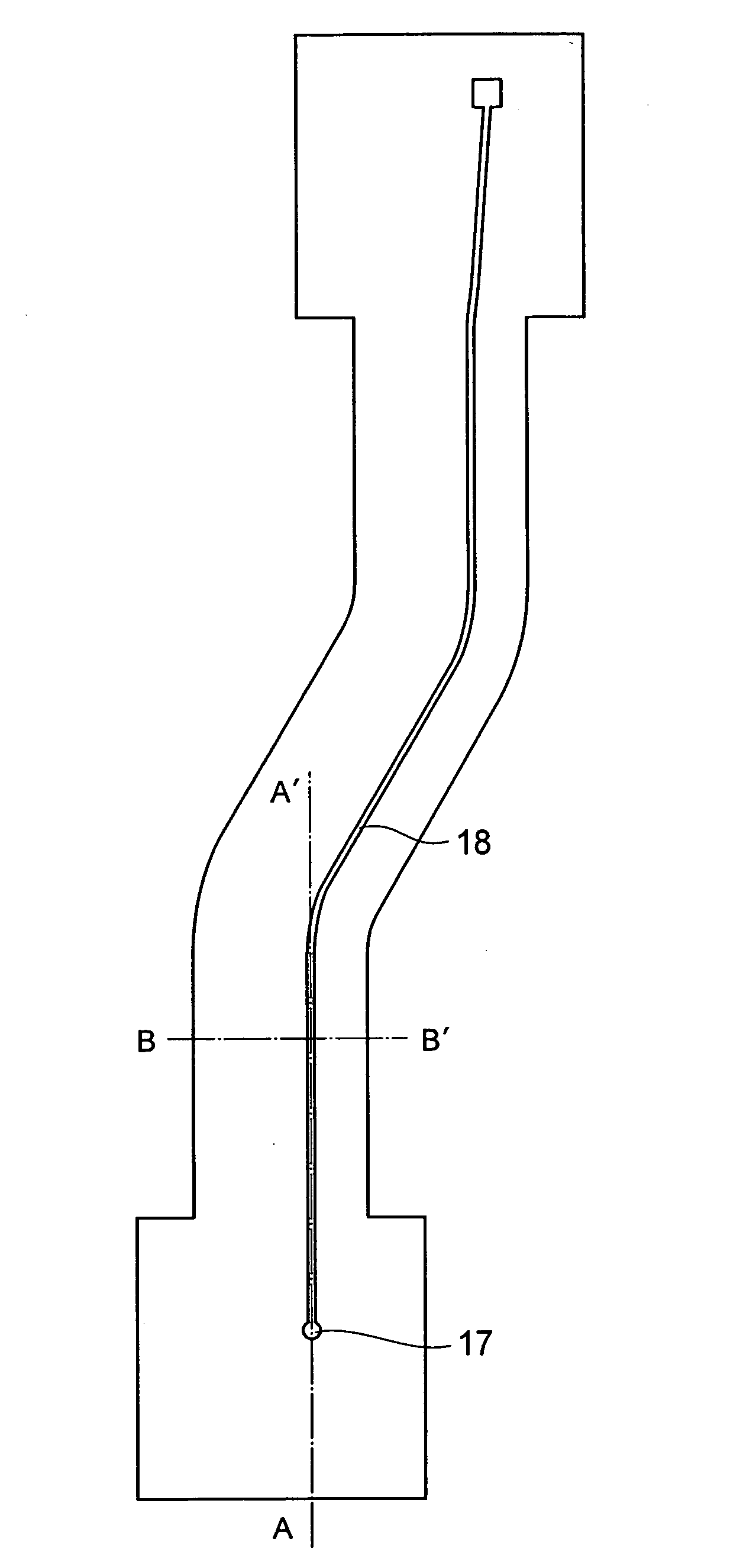
[0063]FIG. 4 is a plan view according to a third embodiment of the present invention. FIGS. 5A and 5B are sectional views taken along line A-A′ and line B-B′ in FIG. 4, respectively.

[0064]First, as shown in FIG. 5A(1), a double-sided copper-clad laminate 16 with a copper foil thickness of 4 μm is prepared. Available materials include double-sided copper-clad laminate Metaloyal PI-25D-CCW-04D0 (#25) (manufactured by Toyo Metallizing Co., LTD.) for the reasons shown in the first embodiment.

[0065]Next, as shown in FIG. 5A(2), a hole 17 for use as a via for interlayer connection is formed. It does not matter whether the via is a through-hole or blind hole. Regarding methods for forming the hole, examples include mechanical drilling, punching, laser drilling, plasma processing, and chemical etching in the case of a through-hole, or examples include laser drilling, plasma processing, and chemical etching in the case of a blind hole. In this embodiment, a through-hole with a diameter of 50...


PUM


Abstract

The present invention provides a microstrip line for a printed wiring board such as a flexible printed wiring board which includes a sandwiched thin insulating layer and cannot use a solid grounding conductor, the microstrip line being such that shape of grounding conductors relative to signal lines remains unchanged even in the presence of a curved shape and that overlapping areas of signal lines and grounding conductors located opposite to each other remain unchanged even in case of exposure misalignment or stack misalignment. A printed wiring board with a microstrip line structure in which signal lines are curved include wire-type grounding conductors 5, 9, 12, 15, 19, or 26 located across an insulating layer 3, 10, or 13 from the signal lines 4, 6, 8, 11, 14, 18, or 25, characterized in that wiring pitch of the grounding conductors is 1 / n of width of the signal lines (where n is a natural number of 1 or 2).

Description

TECHNICAL FIELD[0001]The present invention relates to a printed wiring board, and more particularly, to a structure of a printed wiring board used to transmit high-speed signals to meet the needs for size reduction and performance improvement of electric and electronic equipment.BACKGROUND ART[0002]Recently, signal processing speed of electronic equipment has been getting faster and faster. Consequently, transmission speed of signals passing through printed wiring boards has been increasing as well. In high-speed signal transmission, it is necessary to match characteristic impedance of signal lines, and mismatch will cause signal reflection, resulting in losses.[0003]Generally, the characteristic impedance is 50Ω in the case of a single-ended channel, and 50Ω per signal line in the case of a differential channel. To obtain desired impedance, printed wiring boards which handle high-speed signals use a microstrip line in which a signal line 1 and grounding conductor 2 oppose each othe...

Claims


Application Information

Patent Timeline
IPC IPC(8): H01P3/08H05K1/00
CPCH05K1/0224H05K1/0245H05K2201/09272H05K1/0393H05K2201/09236H05K1/0253H05K1/02
Inventor TOYOSHIMA, RYOICHI
Owner NIPPON MEKTRON LTD
Why Eureka
Try Eureka