Method of manufacturing semiconductor device

Inactive Publication Date: 2010-07-29
SUCCESS INT CORP +1
View PDF4 Cites 11 Cited by
  • Summary
  • Abstract
  • Description
  • Claims
  • Application Information

AI Technical Summary

Benefits of technology

[0008]To attain the aforementioned object, a method of manufacturing a semiconductor device according to the first invention is characterized by including: forming a notched part by dicing from a surface to a middle in a semiconductor substrate and fixing the surface of the semiconductor substrate to a substrate support base; grinding a back surface of the semiconductor substrate to thin the semiconductor substrate; depositing a metal layer on the back surface of the semiconductor substrate and forming a diamond-like carbon film or an amorphous carbon film (hereinafter referred to as “carbon film”) that is a heat receiving layer on the metal layer; irradiating a surface of the carbon film with light at a power density of 1 kW / cm2 to 1 MW / cm2 for a short time of 0.01 ms to ms to heat treat the metal layer and a semiconductor in contact with the metal layer at a predetermined temperature; and separating the semiconductor substrate at the notched part into pieces.
[0009]A method of manufacturing a semiconductor device according to the second invention is characterized by including: fixing a surface of the semiconductor substrate to the substrate support base and then grinding and etching a back surface of the semiconductor substrate to thin the semiconductor substrate; depositing a metal layer on the back surface of the semiconductor substrate and forming a diamond-like carbon film or an amorphous carbon film (hereinafter referred to as “carbon film”) that is a heat receiving layer on the metal layer; irradiating a surface of the carbon film with light at a power density of 1 kW / cm2 to 1 MW / cm2 for a short time of 0.01 ms to ms to heat treat the metal layer and a semiconductor in contact with the metal layer at a predetermined temperature; and dicing from the back surface and separating the semiconductor substrate into pieces.
[0017]As described above, according to the present invention, the steps of thinning a semiconductor substrate by grinding; forming a metal film on the semiconductor substrate thinned; and heat-treating the substrate to improve a contact characteristic are performed with the semiconductor substrate being attached to a substrate support base, unlike a method of the related art where a substrate having been thinned is handled to perform metal formation and heat treatment to improve a contact characteristic. Therefore, the series of steps may be performed without cracks occurred in the substrate. The semiconductor substrate may be easily separated into pieces thereafter.
[0018]In the present invention, a thin (for example, about 0.2 μm-thick) carbon film is formed on a metal layer after depositing the metal layer on a back surface of a semiconductor substrate. The carbon film is an excellent heat absorbing material against light irradiation. The carbon film having an optical absorbance of 40% as a light absorption characteristic may be easily formed in the range of 400 nm to 1000 nm in wavelength depending on a deposition method and a deposition condition for the carbon film. In the case where strong flash lamp light or laser light is applied onto this structure in a related art method, since a metal electrode is exposed on an outermost surface and the metal generally has an extremely high light reflectance, most of incident light energy is lost as reflected light and may not contribute to the improvement in a contact characteristic at the interface between semiconductor and metal. On the other hand, in the present invention, extremely efficiently incident light energy is absorbed in the carbon film and converted into thermal energy, and this energy may improve a contact characteristic between the semiconductor and the metal. Therefore, the energy for this heat process may be easily saved.
[0019]Further, heat treatment in a furnace according to a related art method needs 30 minutes or more. However, according to the present invention, the treatment for the whole substrate surface may be completed by light irradiation for an extremely short time, thereby reducing a process time considerably.
[0020]Accordingly, the yield in a process of manufacturing a semiconductor element using a thin semiconductor substrate having a metal contact on a back surface may be improved using the manufacturing method of the present invention. Steps of the manufacturing process may also be reduced considerably. This may be a great advance in the field of power devices or the like having a substrate with a thickness of 100 μm or less. Accordingly, on-resistance of a semiconductor element such as a power MOS transistor can be reduced, so that energy saving during operation of the element can be achieved.

Problems solved by technology

During this process, the thinned substrate is extremely difficult to be handled, damages such as cracks tend to occur in the substrate and a yield is reduced; this has been a huge problem.

Method used


Image

  • Method of manufacturing semiconductor device
  • Method of manufacturing semiconductor device
  • Method of manufacturing semiconductor device

Examples


Embodiment Construction

[0031]An embodiment of the present invention will be described below with reference to drawings. However, the present invention is not limited thereto.

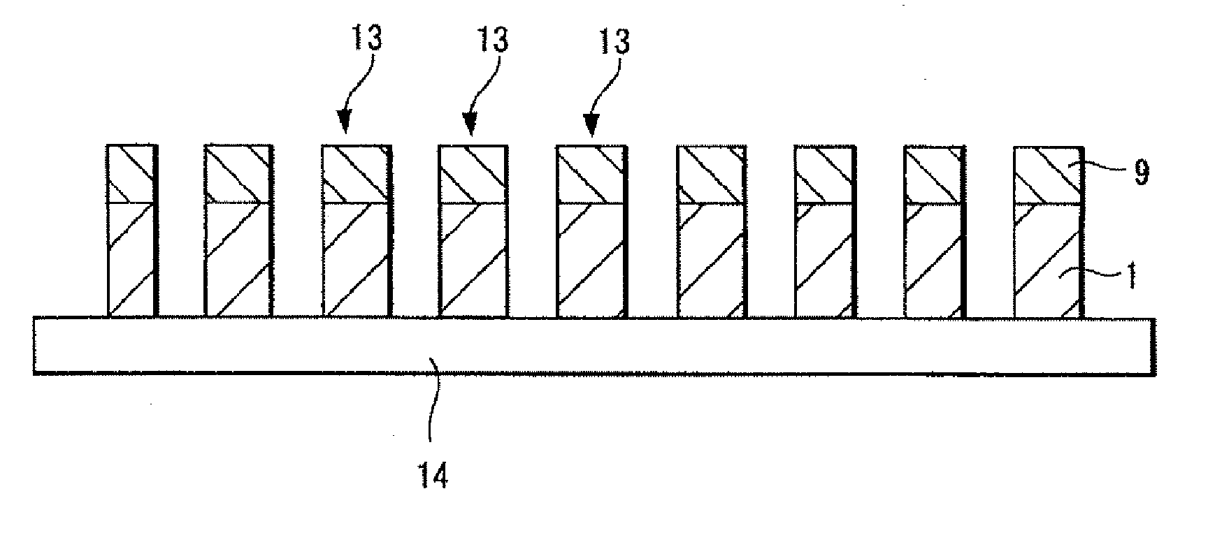
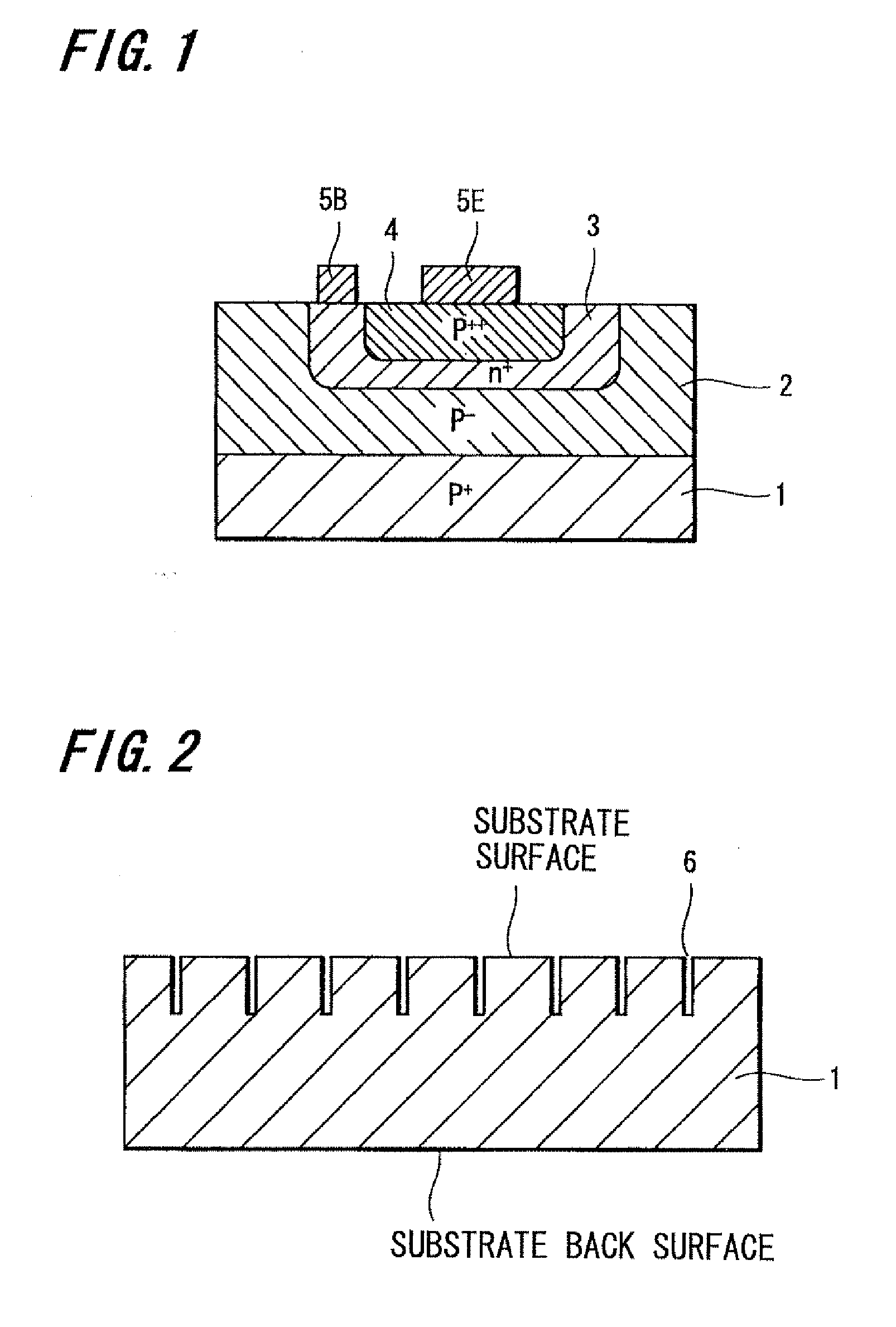
[0032]FIG. 1 shows a schematic cross-sectional view of a semiconductor element having a standard planar pnp transistor structure. There will be described below an embodiment of the manufacturing method of the present invention including a method for heat-treating a semiconductor element having the pnp transistor structure.

[0033]First, a semiconductor element having a pnp transistor structure is formed on a substrate 1 as shown in FIG. 1. A semiconductor substrate, which is here a silicon substrate, is used as the substrate 1. The substrate is not particularly limited in terms of size and may be a typical silicon substrate having a diameter of 200 mm and a thickness of about 500 μm, for example. The semiconductor element (device structure) is formed as a pnp transistor by forming a p− epitaxial layer 2 on the p+ semiconductor substrate...


PUM

PropertyMeasurementUnit
Particle sizeaaaaaaaaaa

Abstract

The present invention provides a method of manufacturing a semiconductor device in which a thinned substrate of a semiconductor or semiconductor device is handled without cracks in the substrate and treated with heat to improve a contact between semiconductor back surface and metal in a high yield and a semiconductor device may be manufactured in a high yield. In the method of manufacturing a semiconductor device according to the present invention, a notched part is formed from a surface to a middle in a semiconductor substrate by dicing and the surface of the substrate is fixed to a support base. Next, a back surface of the substrate is ground to thin the semiconductor substrate and then a metal electrode and a carbon film that is a heat receiving layer are sequentially formed on the back surface of the substrate. Next, the carbon film is irradiated with light at a power density of 1 kW / cm2 to 1 MW / cm2 for a short time of 0.01 ms to 10 ms to transfer heat from the carbon film and alloy an interface between a semiconductor and the metal electrode. Subsequently, the semiconductor substrate is separated at the notched part into pieces.

Description

TECHNICAL FIELD[0001]The present invention relates to a method of manufacturing a semiconductor device. More particularly, the present invention relates to a method of manufacturing a semiconductor device including a process of performing heat treatment to form a metal contact on a semiconductor.BACKGROUND ART[0002]In the manufacture of semiconductor devices such as various semiconductor elements and semiconductor integrated circuits including bipolar transistors and insulated gate field effect transistors (MOS transistors) in the related art, in order to form a contact between semiconductor and metal, a metal layer has usually been deposited on a surface of a semiconductor to receive heat treatment by maintaining them at a predetermined temperature in an annealing furnace in an atmosphere of inert gas or the like for a certain time so that an electric characteristic between the semiconductor and the metal has been improved to obtain an excellent ohmic characteristic (see Patent Doc...

Claims


Application Information

Patent Timeline
IPC IPC(8): H01L21/78
CPCH01L21/268H01L21/28512H01L2924/1305H01L2924/1306B23K26/0051B23K26/0048B23K26/0042B23K26/0012B23K26/0081H01L2924/01075H01L21/6835H01L21/78H01L24/27H01L29/456H01L29/66272H01L2221/68327H01L2221/6834H01L2224/04026H01L2224/27436H01L2924/01013H01L2924/01029H01L2924/01079H01L2924/01322H01L2924/10253H01L2924/13091H01L2924/14H01L2924/01006H01L2924/01023H01L2924/01033H01L2924/01074H01L2924/0132H01L2924/01014H01L2924/3512H01L2924/00B23K26/0006B23K26/354B23K2101/34B23K2101/35B23K2103/08B23K2103/10B23K2103/172B23K2103/56H01L21/28B23K26/60H01L29/41H01L21/26
Inventor KAWANA, YOSHIYUKISANO, NAOKI
Owner SUCCESS INT CORP
Why Eureka
Try Eureka