
Lithographic processing method, and device manufactured thereby

a technology of lithographic processing and processing method, applied in the field of resolution enhancement techniques of photolithography, can solve the problems of incomplete solution of selective bias, negative impact of “best” bias to give identical cd vs. pitch, and reducing rather than enlarging focus

Inactive Publication Date: 2010-07-01
ASML NETHERLANDS BV
View PDF5 Cites 11 Cited by
  • Summary
  • Abstract
  • Description
  • Claims
  • Application Information

AI Technical Summary

Benefits of technology

The present invention provides a method for simulating a photolithography process using a mask layout to produce a first simulated resist image. The method includes perturbing each edge segment in the mask layout by a selected amount to produce an initial perturbed layout, simulating the photolithography process using the initial perturbed layout to produce a second simulated resist image, determining a difference resist image value between the first and second simulated resist images for each edge segment, creating an n×n matrix J based on the difference resist image values and the perturbed amount, initializing the matrix J using the difference in resist image values divided by the perturbed amount, determining a correction delta vector by minimizing the difference resist image values divided by the perturbed amount, perturbing each edge segment in the perturbed layout by the corresponding correction delta vector to create a further perturbed layout, simulating the photolithography process using the further perturbed layout to produce a third simulated resist image, using information from the third simulated resist image and the matrix J to produce an updated matrix J, and updating the correction delta vector by minimizing the difference resist image values divided by the updated matrix J. The invention also provides a computer-readable medium and a litho cell system for performing the method. The technical effects include improving the accuracy and efficiency of the photolithography process.

Problems solved by technology

Selective bias is an incomplete solution to the problem of proximity effects, particularly if it is only applied at the nominal process condition.
Therefore, the “best” bias to give identical CD vs. pitch may even have a negative impact on the overall process window, reducing rather than enlarging the focus and exposure range within which all of the target features print on the wafer within the desired process tolerance.
This type of line end pull back can result in catastrophic failure of the devices being manufactured if the line end fails to completely cross over the underlying layer it was intended to cover, such as a polysilicon gate layer over a source-drain region.
Since this type of pattern is highly sensitive to focus and exposure, simply biasing the line end to be longer than the design length is inadequate because the line at best focus and exposure, or in an underexposed condition, would be excessively long, resulting either in short circuits as the extended line end touches neighboring structures, or unnecessarily large circuit sizes if more space is added between individual features in the circuit.
Since one of the key goals of integrated circuit design and manufacturing is to maximize the number of functional elements while minimizing the area required per chip, adding excess spacing is a highly undesirable solution.
Even at best focus and exposure these extra structures are not clearly resolved and they alter the appearance of the main feature without being fully resolved on their own.
Often referred to as “scattering bars,” this type of sub-resolution assist feature (SRAF) adds yet another layer of complexity to a mask.
The simple task of biasing a one-dimensional line becomes increasingly complicated as two-dimensional structures must be moved, resized, enhanced with assist features, and possibly phase-shifted without causing any conflict with adjoining features.
Due to the extended proximity range of deep sub-wavelength lithography, changes in the type of OPC applied to a feature can have unintended consequences for another feature located within half a micron to a micron.
Since there are likely to be many features within this proximity range, the task of optimizing OPC decoration becomes increasingly complex with the addition of more aggressive approaches.
Such a straightforward correction function does not work well for nonlinear processes because changes on the mask are not linearly reflected in the printed resist image.
In a particular application, the method of calculating the appropriate correction tends to be much more complex, and the correction algorithms can depend on factors such as linewidth error, fabrication process, correction goals, and constraints.
As feature size decreases, solving for the correction amount for individual edge segments experiences convergence problems.

Method used


Image

  • Lithographic processing method, and device manufactured thereby
  • Lithographic processing method, and device manufactured thereby
  • Lithographic processing method, and device manufactured thereby

Examples


Embodiment Construction

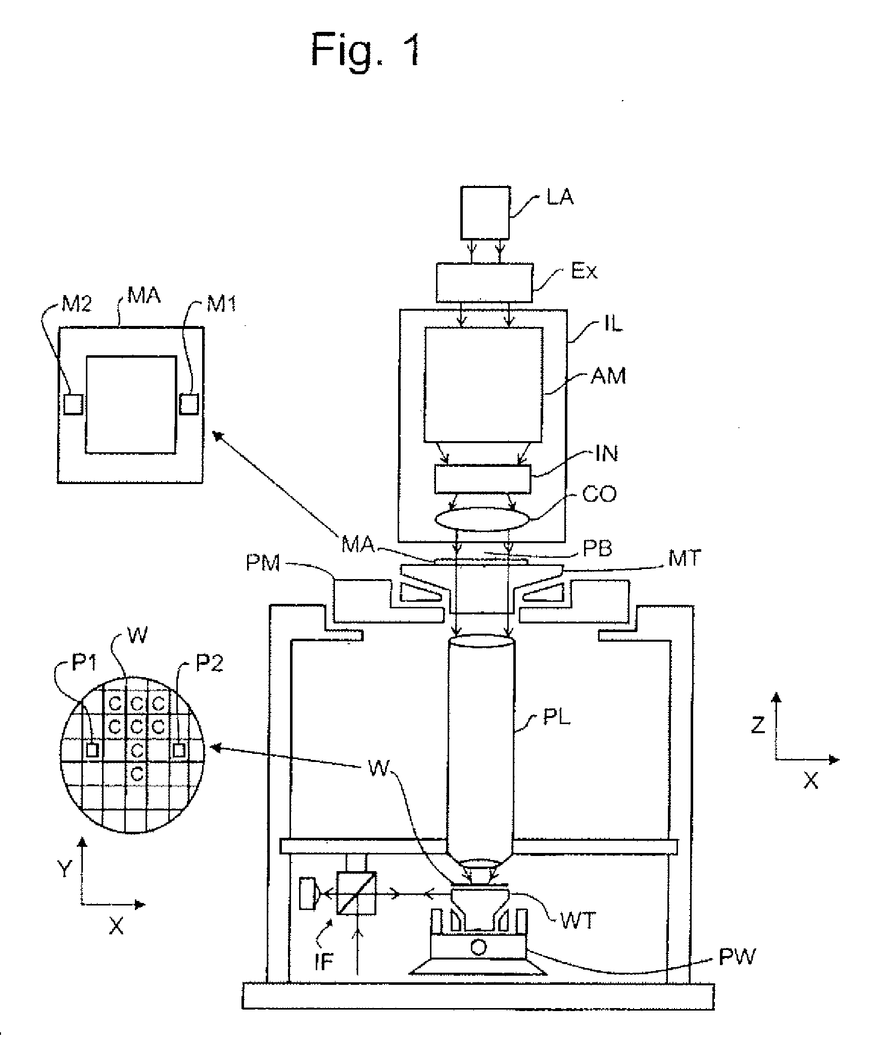
[0044]Although specific reference may be made in this text to the use of lithographic apparatus in the manufacture of ICs, it should be understood that the lithographic apparatus described herein may have other applications, such as the manufacture of integrated optical systems, guidance and detection patterns for magnetic domain memories, liquid-crystal displays (LCDs), thin-film magnetic heads, etc. The skilled artisan will appreciate that, in the context of such alternative applications, any use of the terms “wafer” or “die” herein may be considered as synonymous with the more general terms “substrate” or “target portion,” respectively. The substrate referred to herein may be processed, before or after exposure, in for example a track (a tool that typically applies a layer of resist to a substrate and develops the exposed resist) or a metrology or inspection tool. Where applicable, the disclosure herein may be applied to such and other substrate processing tools. Further, the sub...


PUM

PropertyMeasurementUnit
photosensitiveaaaaaaaaaa
refractive indexaaaaaaaaaa
shapeaaaaaaaaaa

Abstract

A multivariable solver for proximity correction uses a Jacobian matrix to approximate effects of perturbations of segment locations in successive iterations of a design loop. The problem is formulated as a constrained minimization problem with box, linear equality, and linear inequality constraints. To improve computational efficiency, non-local interactions are ignored, which results in a sparse Jacobian matrix.

Description

CROSS-REFERENCE TO RELATED APPLICATIONS[0001]The present invention claims priority from U.S. Provisional Patent application No. 61 / 141,298, entitled “Lithographic Processing Method, and Device Manufactured Thereby” filed Dec. 30, 2008.BACKGROUND OF THE INVENTION[0002]1. Field of the Invention[0003]The present invention relates generally to resolution enhancement techniques for photolithography and more particularly to techniques for optical proximity correction.[0004]1. Description of the Related Art[0005]A lithographic apparatus is a machine that applies a desired pattern onto a target portion of a substrate. The apparatus generally comprises a radiation system for supplying a beam of radiation, a support structure for supporting a patterning device, the patterning device serving to pattern the beam, a substrate table for holding a substrate, and a projection system for projecting the patterned beam of radiation onto a target portion of the substrate. Lithographic apparatus can be ...

Claims


Application Information

Patent Timeline
Patent Type & Authority Applications(United States)
IPC IPC(8): G03F1/00G06F17/50
CPCG03F1/36
Inventor WONG, WILLIAM S.LIU, FEICHEN, BEEN-DERLU, YEN WEN
Owner ASML NETHERLANDS BV
Learn More