
Semiconductor device and its manufacturing method

Inactive Publication Date: 2010-07-01
SANKEN ELECTRIC CO LTD
View PDF3 Cites 4 Cited by
  • Summary
  • Abstract
  • Description
  • Claims
  • Application Information

AI Technical Summary

Benefits of technology

[0033]With the present invention having the above configuration, it is possible to reduce on-state resistance and increases reliability in the semiconductor device having an electrode formed in the recessed structure.

Problems solved by technology

Therefore, it is not easy to reduce a variation of the contact resistance or resistance value.
When the positions of the electrode 205 and recessed region 207 are displaced from each other due to poor accuracy of the alignment, contact between the electrode 205 and two-dimensional electron gas layer becomes incomplete in some cases, which may accordingly increase the resistance of this portion to degrade the reliability of the device.
Further, in the case of the structure of Patent Document 1, current concentrates on the portion at which the interval between the concavities and convexities on the edge surface of the recessed region in the source and concavities and convexities on the edge surface of the recessed region in the drain becomes small, causing a reduction in reliability on prolonged use.
Thus, in a semiconductor device having an electrode formed in the recessed structure, it has been difficult to reduce the on-state resistance and increase reliability of the device.

Method used


Image

  • Semiconductor device and its manufacturing method
  • Semiconductor device and its manufacturing method
  • Semiconductor device and its manufacturing method

Examples


first embodiment

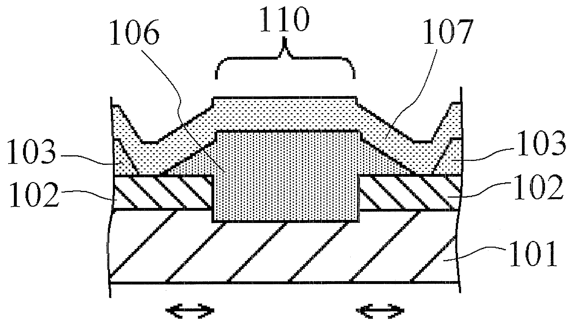
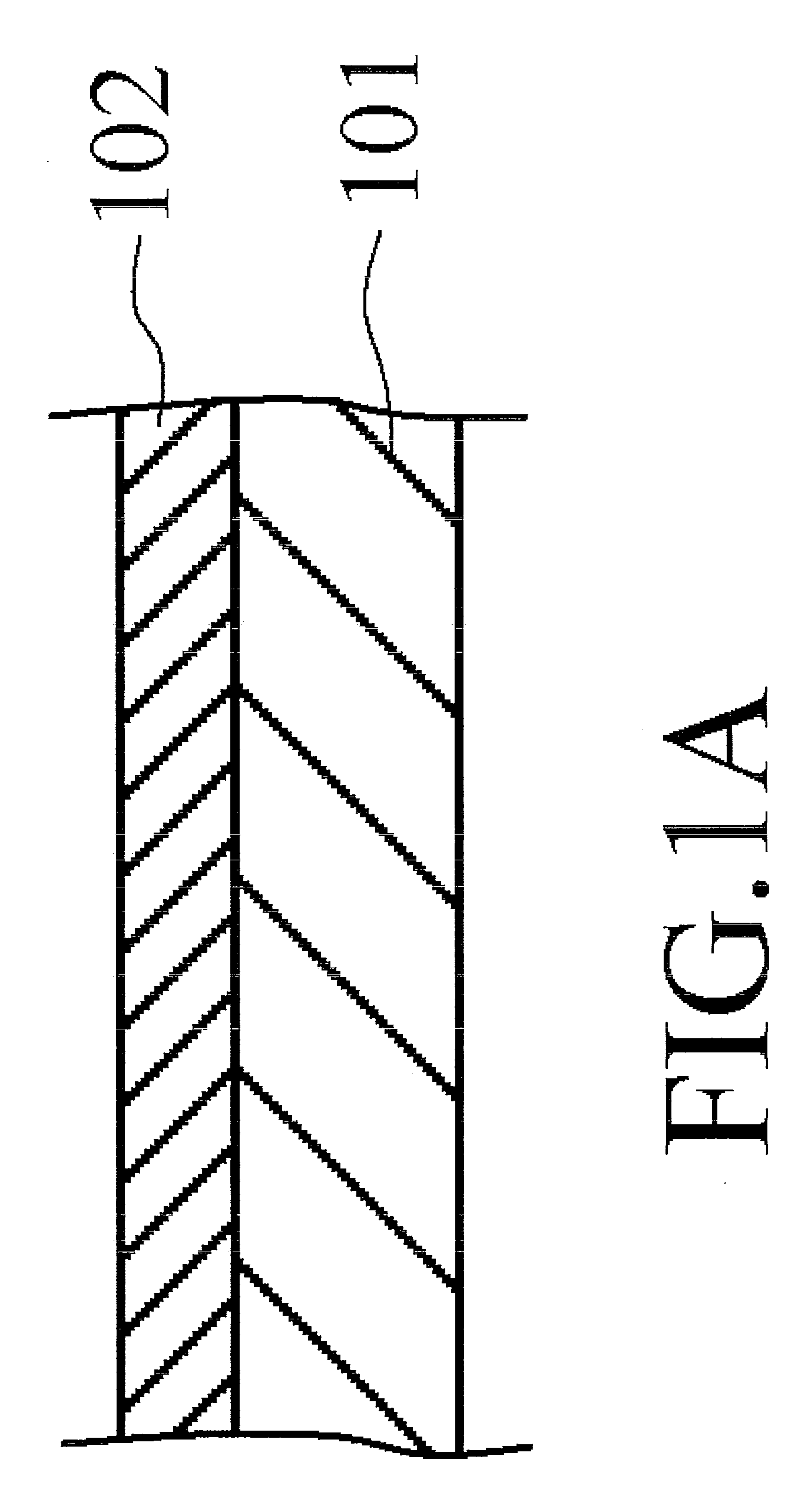
[0041]FIGS. 1A to 1I are process cross-sectional views of a structure around the source or drain of the manufacturing method according to a first embodiment. In the first step of the manufacturing method of this HEMT, a laminated semiconductor structure (semiconductor layer) in which an AlGaN layer 102 serving as a carrier supply layer is formed on a GaN layer 101 serving as a channel layer by a MOCVD (Metal Organic Chemical Vapor Deposition) method is produced as illustrated in FIG. 1A. Although the GaN layer 101 is formed on a silicon substrate through a buffer layer as in the case illustrated in FIG. 5, the illustration thereof is omitted here. The silicon substrate is a monocrystalline silicon substrate having a sufficient size. The buffer layer is used as needed for forming the GaN layer 101 with a less crystal defect on the silicon substrate having a lattice constant different from that of GaN. The buffer layer may be formed in a multilayered structure. The formation of the bu...

second embodiment

[0057]It is apparent that the same effect can be obtained even when the insulating layer side etching process is performed after the lithography process (after the formation of the photoresist pattern 104) and before the semiconductor etching process (before forming recessed region 110 in AlGaN layer 102 and GaN layer 101) in the above manufacturing method. FIGS. 3A to 3H are process cross-sectional views illustrating a manufacturing method obtained by changing a part of the manufacturing method according to the first embodiment in this point of view. In the manufacturing method according to the present embodiment, the entire process has been further simplified as compared to the manufacturing method according to the first embodiment.

[0058]FIGS. 3A, 3B, and 3C are the same as FIGS. 1A, 1B, and 1C in the manufacturing method according to the first embodiment, and the descriptions thereof are omitted here.

[0059]In FIG. 3D, the first insulating layer 103 is etched using the photoresist...


PUM


Abstract

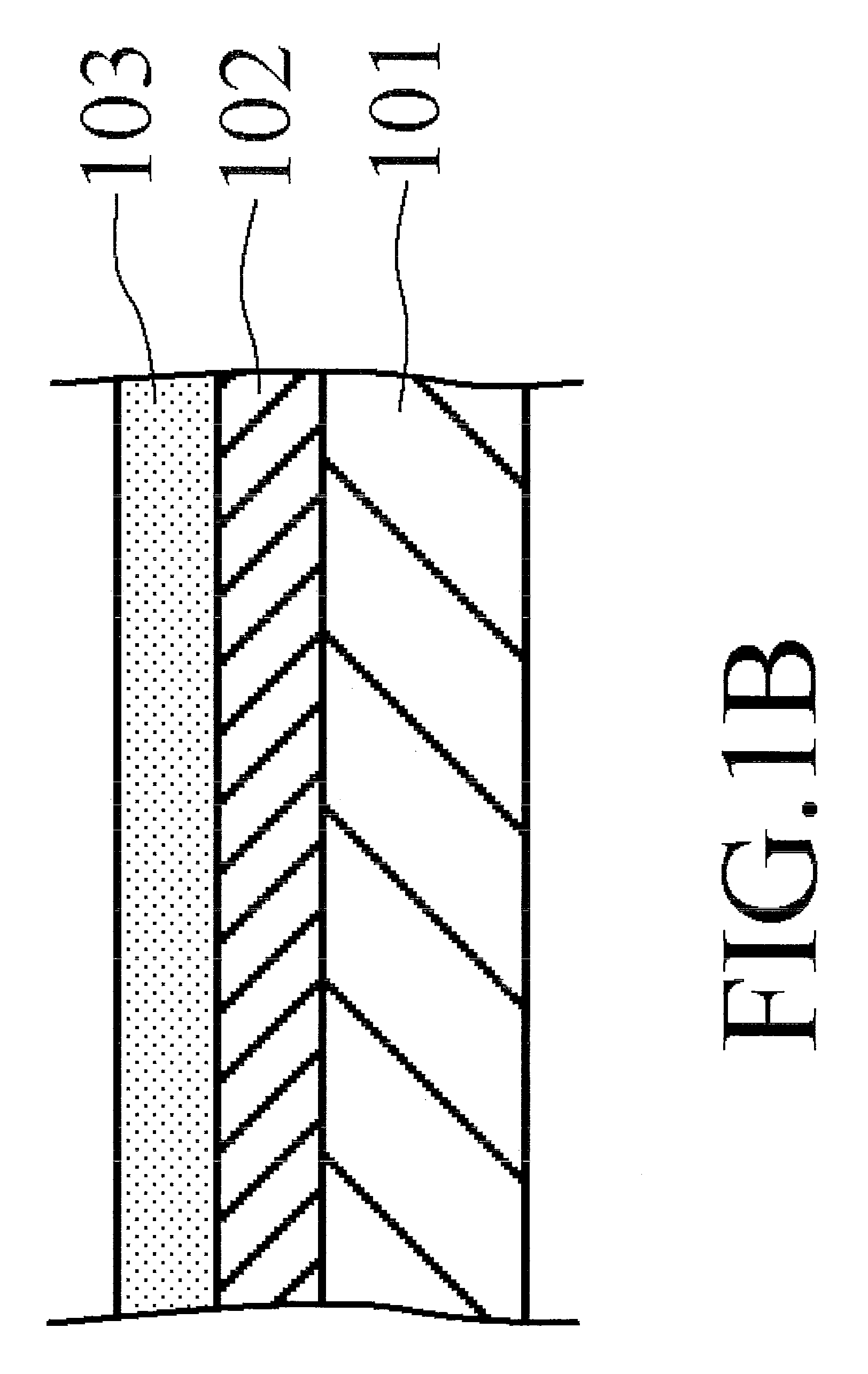
An object of the present invention is to reduce on-state resistance and increases reliability in a semiconductor device having an electrode formed in a recessed structure.As illustrated in FIG. 1B, a first insulating layer 103 is formed. Then, as illustrated in FIG. 1C, a photolithography process is carried out to form a photoresist pattern 104. Subsequently, as illustrated in FIG. 1D, dry etching is applied to the first insulating layer 103. Then, as illustrated in FIG. 1E, a laminated semiconductor structure is etched. Next, in this state, wet etching is applied to the first insulating layer 103 as illustrated in FIG. 1F. Next, in this state, an electrode material 105 is formed on the entire exposed surface as illustrated in FIG. 1G. Finally, as illustrated in 1H, the photoresist pattern 104 is removed.

Description

BACKGROUND OF THE INVENTION[0001]1. Field of the Invention[0002]The present invention relates to a semiconductor device manufacturing method and, more particularly, to a manufacturing method of a semiconductor device including an electrode formed in a recessed structure and the semiconductor device.[0003]2. Description of the Related Art[0004]There is known an HEMT (High Electron Mobility Transistor) as a high speed transistor. The HEMT is a transistor capable of operating at high-speed by a configuration where a two-dimensional electron gas is formed in a laminated semiconductor structure by utilizing a compound semiconductor heterojunction so as to increase the mobility of electron. In the HEMT, the two-dimensional electron gas does not flow on the outermost surface in the laminated semiconductor structure but flows near the interface of the laminated semiconductor structure, so that a contact with a drain and a source needs to be formed in the laminated semiconductor structure so...

Claims


Application Information

Patent Timeline
IPC IPC(8): H01L29/778H01L21/283
CPCH01L21/28575H01L29/2003H01L29/41758H01L29/66462H01L29/7787
Inventor KANEKO, NOBUO
Owner SANKEN ELECTRIC CO LTD
Learn More