
Disconnected DPW Structures for Improving On-State Performance of MOS Devices

Active Publication Date: 2009-10-15
TAIWAN SEMICON MFG CO LTD
View PDF3 Cites 12 Cited by
  • Summary
  • Abstract
  • Description
  • Claims
  • Application Information

AI Technical Summary

Benefits of technology

[0009]The advantageous features of the present invention include reduced source-drain on-state resistance and improved on-state drive current performance.

Problems solved by technology

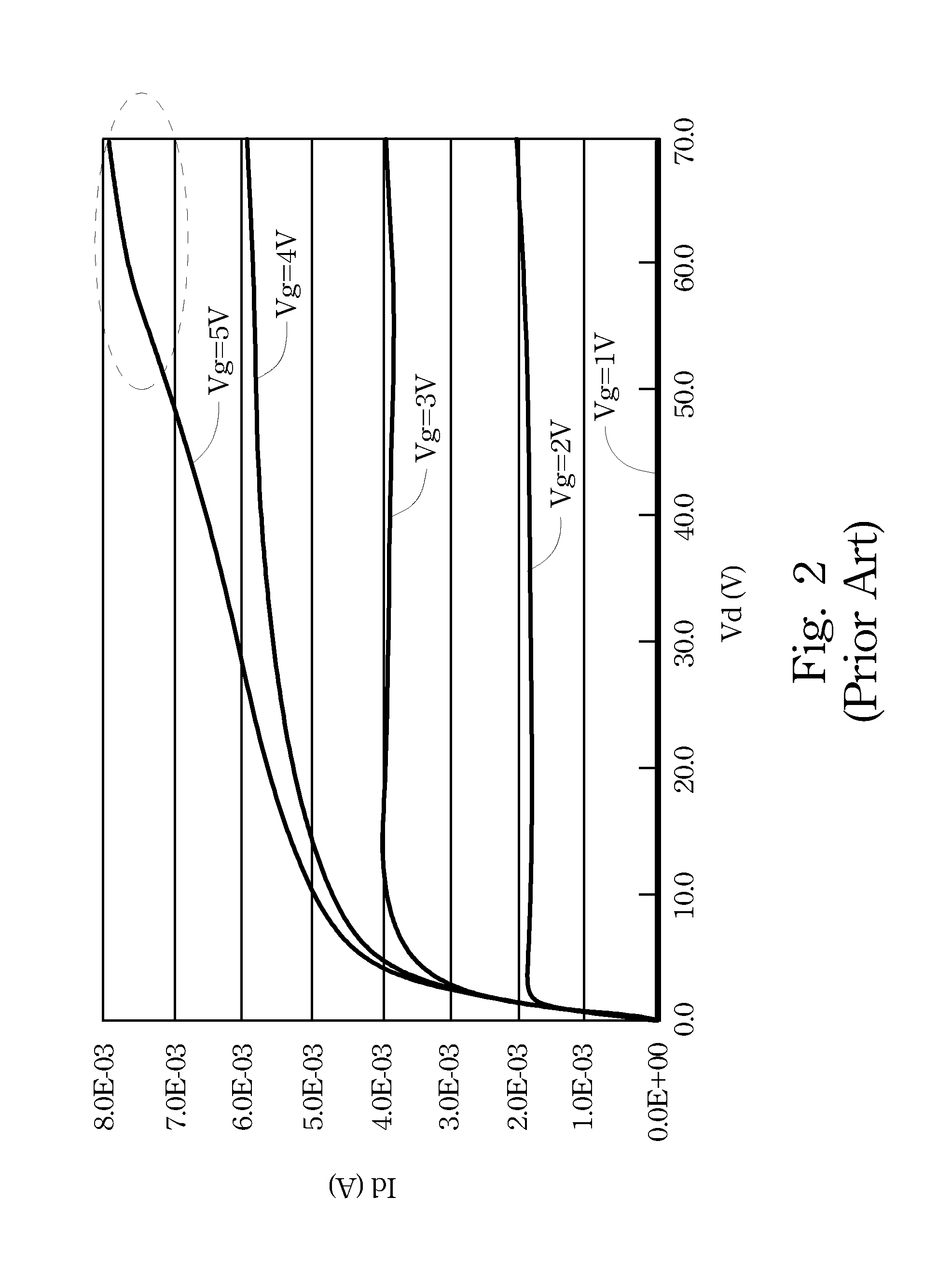
This indicates an output resistance problem, which will cause the degradation in device reliability.
Further, the existing SPICE models cannot simulate such a device behavior.

Method used


Image

  • Disconnected DPW Structures for Improving On-State Performance of MOS Devices
  • Disconnected DPW Structures for Improving On-State Performance of MOS Devices
  • Disconnected DPW Structures for Improving On-State Performance of MOS Devices

Examples


Embodiment Construction

[0016]The making and using of the presently preferred embodiments are discussed in detail below. It should be appreciated, however, that the present invention provides many applicable inventive concepts that can be embodied in a wide variety of specific contexts. The specific embodiments discussed are merely illustrative of specific ways to make and use the invention, and do not limit the scope of the invention.

[0017]A high-voltage metal-oxide-semiconductor (HVMOS) embodiment is described with reference to FIGS. 3 through 10, and variations of the preferred embodiments are then discussed. Throughout the various views and illustrative embodiments of the present invention, like reference numbers are used to designate like elements.

[0018]Referring to FIG. 3, substrate 20 is provided. Substrate 20 is preferably formed of a semiconductor material such as silicon, or other commonly used semiconductor materials such as SiGe and / or other group III, group IV, and / or group V elements. Prefera...


PUM


Abstract

A semiconductor structure includes a semiconductor substrate; a first high-voltage well (HVW) region of a first conductivity type overlying the semiconductor substrate; a second HVW region of a second conductivity type opposite the first conductivity type overlying the substrate and laterally adjoining the first HVW region; a gate dielectric extending from over the first HVW region to over the second HVW region; a gate electrode on the gate dielectric; a drain region in the second HVW region; a source region at an opposite side of the gate dielectric than the drain region; and a deep well region of the first conductivity type underlying the second HVW region. Substantially no deep well region is formed directly underlying the drain region.

Description

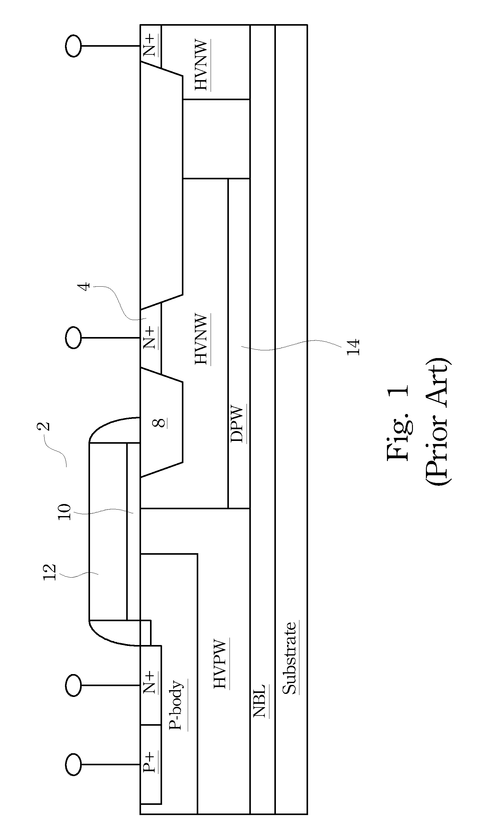
TECHNICAL FIELD[0001]This invention relates generally to semiconductor devices, and more particularly to metal-oxide-semiconductor (MOS) devices, and even more particularly to the structure and manufacturing methods of high-voltage MOS devices.BACKGROUND[0002]High-voltage metal-oxide-semiconductor (HVMOS) devices are widely used in many electrical devices, such as input / output (I / O) circuits, CPU power supplies, power management systems, AC / DC converters, etc.[0003]There are a variety of forms of HVMOS devices. A symmetric HVMOS device may have a symmetric structure on the source side and drain side. High voltages can be applied on both drain and source sides. An asymmetric HVMOS device may have asymmetric structures on the source side and drain side. For example, only one of the source side and drain side, typically the drain side, is designed for sustaining high voltages.[0004]FIG. 1 illustrates a conventional asymmetric HVNMOS device 2, which includes gate oxide 10, gate electrod...

Claims


Application Information

Patent Timeline
IPC IPC(8): H01L29/78
CPCH01L29/0623H01L29/063H01L29/0653H01L29/0847H01L29/0878H01L29/1045H01L29/7836H01L29/66659H01L29/66689H01L29/7816H01L29/7833H01L29/7835H01L29/1095
Inventor CHIANG, PUO-YULIN, TSAI CHUNHUANG, TSUNG-YI
Owner TAIWAN SEMICON MFG CO LTD
Learn More