
Piezoelectric Frame, Piezoelectric Device and Manufacturing Method for Same

Inactive Publication Date: 2010-06-17
NIHON DEMPA KOGYO CO LTD
View PDF2 Cites 2 Cited by
  • Summary
  • Abstract
  • Description
  • Claims
  • Application Information

AI Technical Summary

Benefits of technology

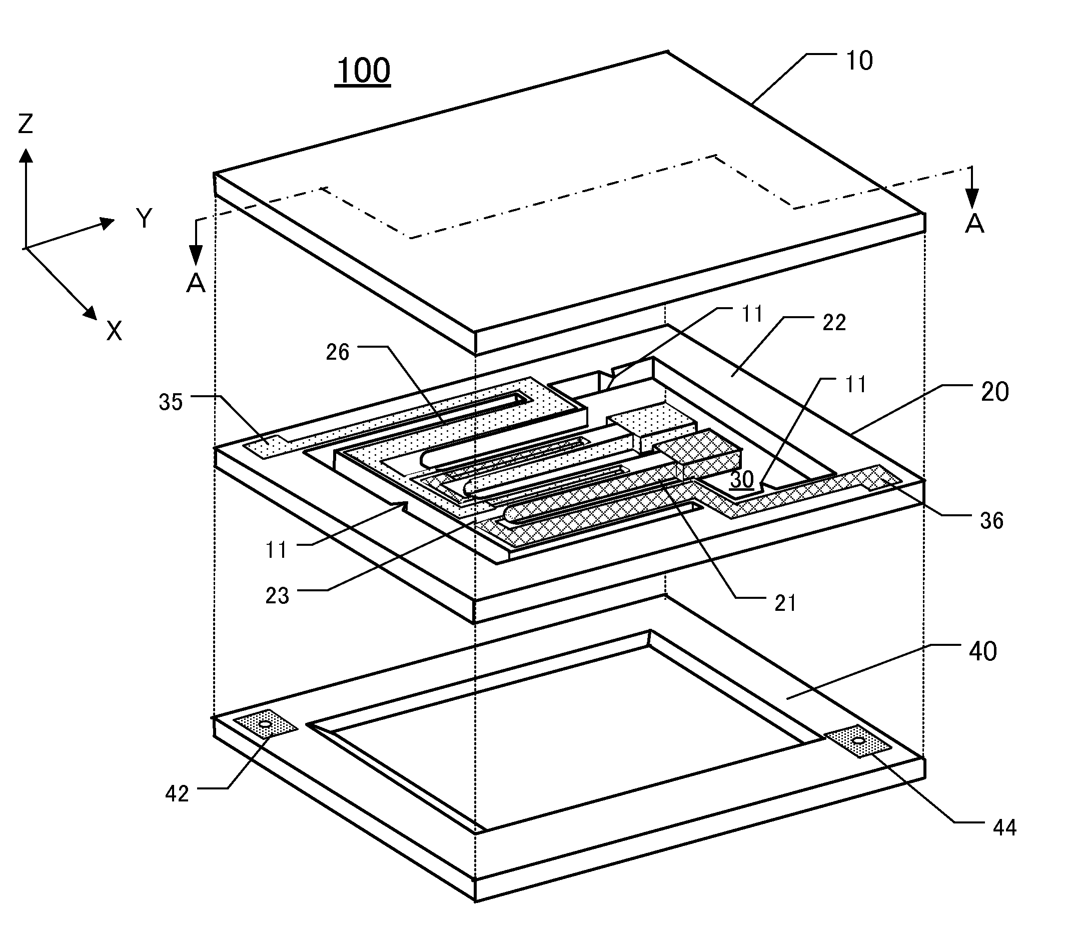
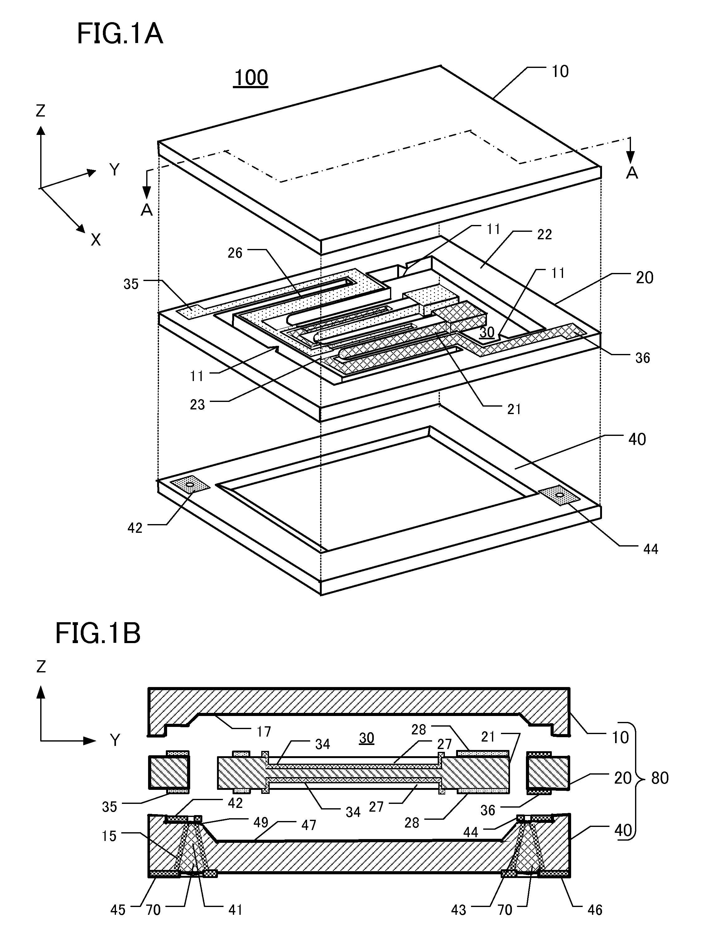
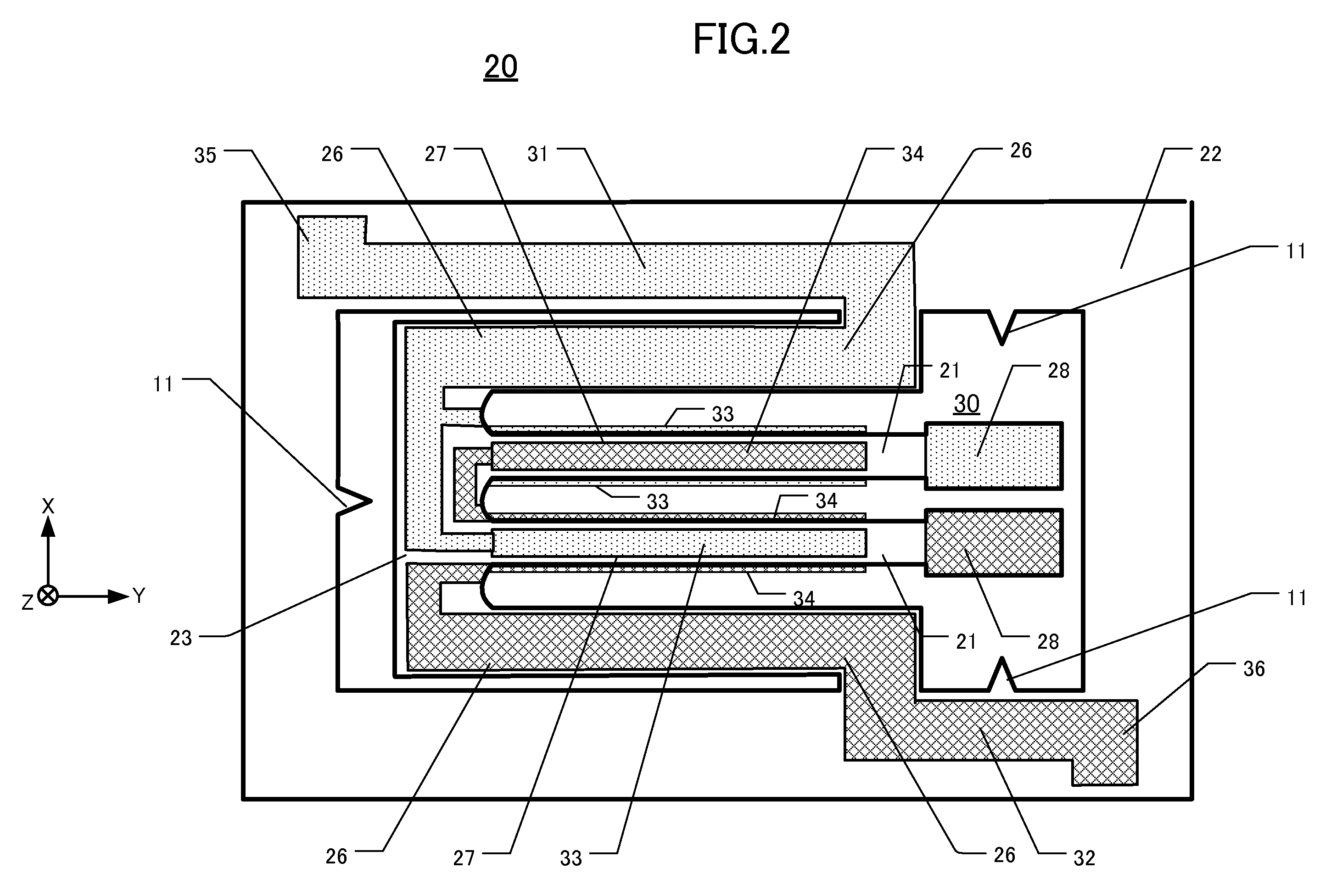
[0009]According to the above-mentioned configuration, an acute angle portion is formed between the outer frame portion and the tuning-fork type piezoelectric vibrating piece. The acute angle portion reflects exposing light vertically coming in Z-direction for forming electrodes. Thus, when the electrodes are formed, exposing light is sufficiently irradiated to the side surface where the photoresist film is applied. Then the electrode films formed on the side surfaces of the acute angle portion and piezoelectric frame are removed by etching and the electrode patterns formed thereby are not prone to short-circuit.
[0015]By using the above-mentioned piezoelectric frame, piezoelectric devices having less failure caused by short-circuiting of electrodes can be provided.
[0020]Piezoelectric devices constructed according to the present disclosure prevent failures caused by short-circuiting of piezoelectric frames or devices induced by the remainder of metal film due to insufficient exposure to light during processing, eliminating the need for physical removal of metal film.

Problems solved by technology

When forming connecting terminals for a piezoelectric vibrating piece and forming electrical conductors on side surfaces of a piezoelectric vibrating piece, misalignment of a mask or flowing of deposition metal may happen.
As a result, unwanted metal adheres to areas of the connecting terminals and it may cause short-circuit.
Also, spaces between adjacent side surfaces of a base portion, side surfaces of a frame, and side surfaces of a piezoelectric vibrating piece are narrow because of miniaturization, so that exposure of photoresist material can be incomplete.
This can also result in unwanted remains of metal film which can cause short-circuits.
In this way, short-circuits caused by remaining metal film on side surfaces of structures in a miniaturized piezoelectric vibrating device are a typical cause of product failure.
Also, this cutting process requires detail-related work so that can slow mass production or increase the costs of production.

Method used


Image

  • Piezoelectric Frame, Piezoelectric Device and Manufacturing Method for Same
  • Piezoelectric Frame, Piezoelectric Device and Manufacturing Method for Same
  • Piezoelectric Frame, Piezoelectric Device and Manufacturing Method for Same

Examples


second embodiment

Configuration of Second Crystal Frame 20A

[0048]FIG. 3 is a top view of a second crystal frame 20A. A difference between the first crystal frame 20 of the first embodiment and the second crystal frame 20A of the second embodiment is that a concave portion having a first acute angle is formed on the side surface of the outer frame portion 22. The same numberings are used for the same members of the first embodiment and only differences will be explained.

[0049]The second crystal frame 20A is provided with a concave portion 12 having a first acute angle at the side surface of the outer frame portion 22. The concave portion 12 takes a form of an acute angle when it is seen from Z-direction. The concave portion 12 having a first acute angle is formed on the side surface of the outer frame portion and faces the tuning-fork crystal vibrating piece 30. In FIG. 3, the concave portion 12 having a first acute angle formed on the left side is formed within a range from the base portion 23 to the...

third embodiment

Configuration of Second Crystal Frame 20B

[0050]FIG. 4 is a top view of a third crystal frame 20B. A difference between the first crystal frame 20 of the first embodiment and the third crystal frame 20B of the third embodiment is that a projection 13 having a second acute angle and a projection 14 having a third acute angle are formed on the side surface of the base portion 23 and the supporting arm 26. The same numberings are used for the same members of the first embodiment and only differences will be explained.

[0051]In FIG. 4, the projections 13 having a second acute angle on the left are formed on the side surface of the base portion 23. Although the projections 13 are formed on the base portion 23, they do not have any effect on oscillation frequency of the tuning-fork type crystal vibrating piece 30. Also, the projections 14 having a third acute angle are formed on the side surface of the supporting arms 26 that face the outer frame portion 22. Although the projections 14 are ...

first example

[0074]FIG. 7A is a top view showing a first photo mask 91-1 for the profile forming of the first crystal frame 20. For a better understanding, the first photo mask 91-1 shows a profile of the mask frame 95 corresponding to the first crystal frame 20 with dotted line. Light shielding portions corresponding to the tuning-fork type crystal vibrating piece 30 the outer frame portion 22, and the supporting arms 26 of the first crystal frame 20 are drawn on the first photo mask 91-1. A light shielding portion 961 corresponding to the projection 11 having a first acute angle is drawn. A plurality of first crystal frame 20 is drawn and for accurate alignments of the single crystal wafer and the photo mask, alignment marks are drawn on the first photo mask 91-1. FIG. 7B is a top view showing a first photo mask 91-2 for the profile forming of the first crystal frame 20. The tuning-fork type crystal vibrating piece 30, the outer frame portion 22, and the supporting arms 26 of the first crystal...


PUM

PropertyMeasurementUnit
Angleaaaaaaaaaa

Abstract

A piezoelectric frame (20) is comprised of a tuning-fork type piezoelectric vibrating piece (30) having a pair of vibrating arms (21) extending from a base portion (23) wherein excitation electrodes are formed on the vibrating arms, an outer frame (22) surrounding the tuning-fork type piezoelectric vibrating piece, a pair of supporting arms (26) extending from the base portion to the outer frame portion and supporting the tuning-fork type piezoelectric vibrating piece; and an acute angle portion (11) formed on a side surface between the outer frame and the tuning-fork type piezoelectric vibrating piece and having an acute angle seen from Z-direction.

Description

CROSS-REFERENCE TO RELATED APPLICATION[0001]This application claims priority to and the benefit of Japan Patent Application No. 2008-321002, filed on Dec. 17, 2008, in the Japan Patent Office, the disclosure of which is incorporated herein by reference in its entirety.FIELD[0002]The present disclosure relates to a piezoelectric frame and methods of manufacturing piezoelectric frames having a reduced likelihood of short circuit failure.DESCRIPTION OF THE RELATED ART[0003]Piezoelectric (crystal) vibrating devices used for mobile communication device and / or OA equipment must be increasingly miniaturized and / or provided with a thin profile or high frequency capability so as to be correspondingly accommodated in electronic devices that likewise are miniaturized. Also, surface mount (SMD: surface mount device) piezoelectric vibrating elements that can be mounted on a circuit board are required.[0004]With miniaturization of piezoelectric vibrating pieces, spaces between conductive elements...

Claims


Application Information

Patent Timeline
IPC IPC(8): G01C19/56H04R17/00H01L41/09H01L41/18H01L41/22H01L41/29H01L41/332H03H3/02H03H9/02
CPCH03H9/0595H03H9/1035Y10T29/42H04R17/00H03H9/21
Inventor ICHIKAWA, RYOICHI
Owner NIHON DEMPA KOGYO CO LTD
Learn More