Manufacturing method of semiconductor device, and semiconductor device

a manufacturing method and technology of semiconductor devices, applied in the direction of printed circuit aspects, sustainable manufacturing/processing, final product manufacturing, etc., can solve the problems of semiconductor devices being discarded as defective goods, electric connection defects, and unfavorable, and achieve the effect of preventing an electric connection d

Inactive Publication Date: 2010-06-10
RENESAS ELECTRONICS CORP
View PDF1 Cites 5 Cited by
  • Summary
  • Abstract
  • Description
  • Claims
  • Application Information

AI Technical Summary

Benefits of technology

[0018]A manufacturing method of a semiconductor device and a semiconductor device according to the present invention make it possible to prevent an electric connection defect due to a solder suction phenomenon (suction). For example, in the case where a solder bump on a semiconductor chip side and a spare solder on a package substrate side are made of same materials and a semiconductor chip is connected to a package substrate by heat-melting the solder bump and the spare solder at the same time, an electric connection defect caused by sucking the spare solder to the solder bump side can be avoided.

Problems solved by technology

However, this is not favorable in consideration of an environmental measure such as a Restriction of the Use of Certain Hazardous Substances in Electrical and Electronic Equipment (RoHS: Restriction of Hazardous Substances) or the like since any of the solder on the chip side and the solder on the substrate side includes lead.
This may generate an electric connection defect.
If the connection defect is generated, this semiconductor device will be discarded as defective goods.
However, in any of the above-mentioned cases, a movement of a solder in melting process, such as a solder suction phenomenon, is not considered.
Generally, in a reflow step, when a solder bump and a spare solder are heat-melted and connected together, the spare bump is sucked by a solder bump side and this may generate an electric connection defect of a solder.

Method used


Image

  • Manufacturing method of semiconductor device, and semiconductor device
  • Manufacturing method of semiconductor device, and semiconductor device
  • Manufacturing method of semiconductor device, and semiconductor device

Examples


Embodiment Construction

[0026]The invention will be now described herein with reference to illustrative embodiments. Those skilled in the art will recognize that many alternative embodiments can be accomplished using the teachings of the present invention and that the invention is not limited to the embodiments illustrated for explanatory purposed.

[0027]Hereinafter, an embodiment of the present invention will be described referring to the attached drawings.

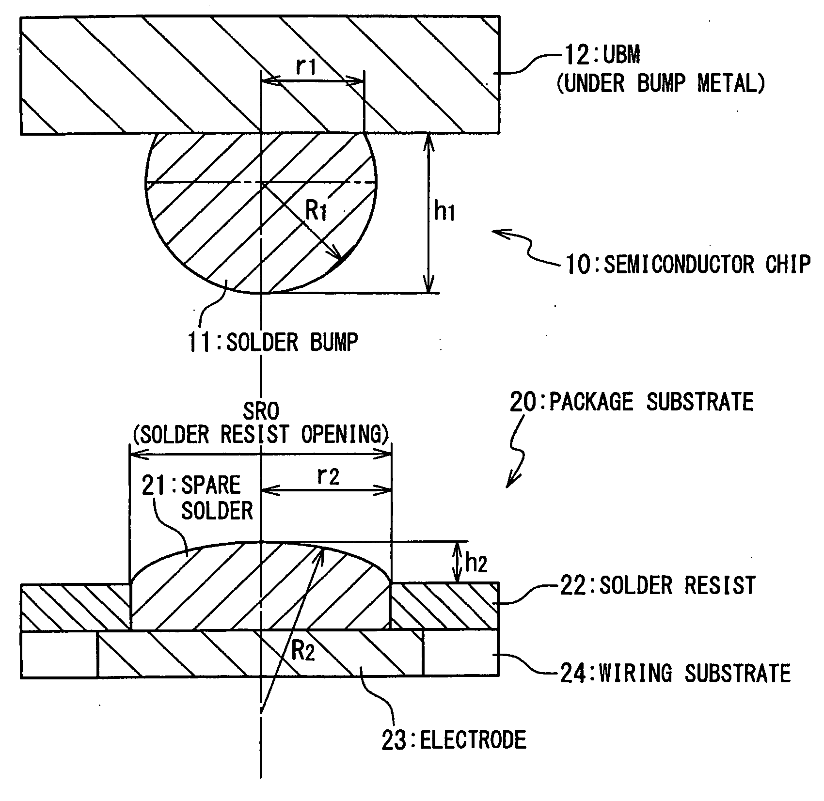
[0028]FIG. 1 shows a configuration example of a semiconductor device according to the embodiment of the present invention.

[0029]The semiconductor device according to the embodiment includes a semiconductor chip 10 and a package substrate 20.

[0030]In this case, it is assumed that the semiconductor device according to the embodiment is a flip-flop type semiconductor device in which the semiconductor chip 10 and the package substrate 20 are connected via solder bumps. As an example of the semiconductor chip 10, a silicon chip (a bare chip) is supposed. As a...


PUM


Abstract

A manufacturing method of a semiconductor device includes a first to fourth steps. The first step includes a step of determining an UBM (Under Bump Metal) radius of an UBM of a chip. The second step includes a step of determining a first curvature radius of a solder bump formed on the UBM. The third step includes a step of determining a SRO (Solider Resist Opening) radius of a SRO of a substrate such that a ratio of the SRO radius to the UMB radius is in a range from 0.8 to 1.2. The fourth step includes a step of determining a second curvature radius of a spare solder formed on an electrode in the SRO such that the second curvature radius is equal to or more than the first curvature radius.

Description

INCORPORATION BY REFERENCE[0001]This application is based upon and claims the benefit of priority from Japanese patent application No. 2008-294635 filed on Nov. 18, 2008, the disclosure of which is incorporated herein in its entirety by reference.BACKGROUND OF THE INVENTION[0002]1. Field of the Invention[0003]The present invention relates to a manufacturing method of a semiconductor device and the semiconductor device. Particularly, the present invention relates to a manufacturing method of a flip-chip type semiconductor device and the flip-chip type semiconductor device.[0004]2. Description of Related Art[0005]According to a typical flip-chip type semiconductor device, a chip is connected to a substrate by using a following method. That is, first, a material is selected, of which melting point is lower than that of a solder bump (a solder ball or the like) located on a chip side, for a spare solder located on a substrate side. Then, when a connection process is carried out between ...

Claims


Application Information

Patent Timeline
Patent Type & Authority Applications(United States)
IPC IPC(8): H01L23/498H01L21/60
CPCH01L23/49811H01L24/05H01L2924/10253H01L24/13H01L24/16H01L24/81H01L2224/81193H01L2224/812H01L2224/81801H01L2924/01078H01L2924/01082H01L2924/01322H05K3/3436H05K3/3452H05K3/3457H05K2201/0379H01L2924/01006H01L2924/01033H01L2924/00H01L2224/0401Y02P70/50
Inventor ISHIDO, KIMINORIINOMATA, TERUJI
Owner RENESAS ELECTRONICS CORP
Why Eureka
Try Eureka