Miniature antenna
- Summary
- Abstract
- Description
- Claims
- Application Information
AI Technical Summary
Benefits of technology
Problems solved by technology
Method used
Image
Examples
second embodiment
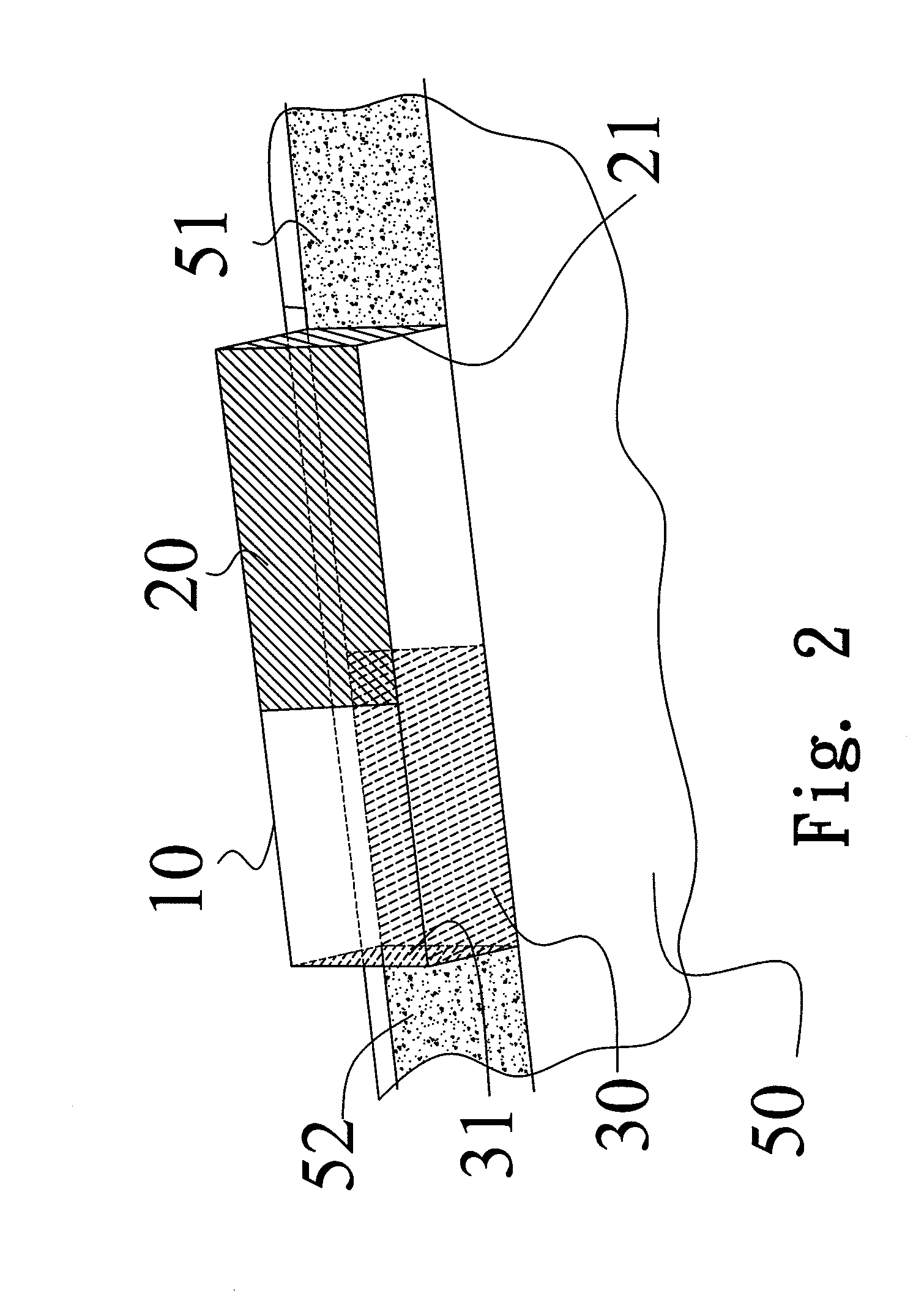
[0029]There are various means to realize the antenna structure disclosed in the present invention, and the present invention does not limit the means to realize the present invention. Further, any structure similar to the structure disclosed in the present invention and having equivalent functions should be also included within the scope of the present invention. FIG. 5(a) to FIG. 5(d) illustrates schematically a thick film process used to realize a plurality of miniature antennas according to the present invention. In FIG. 5(a), a thick film process is used to fabricate a plurality of second electrode layers 30 on a carrier substrate 40. The carrier substrate 40 is made of a ceramic material, a glass material, a polymeric material, or a combination of the abovementioned materials. In FIG. 5(b), a thick film process is used to fabricate dielectric elements 10 on the second electrode layers 30 and the carrier substrate 40. In FIG. 5(c), a thick film process is used to fabricate a plu...
third embodiment
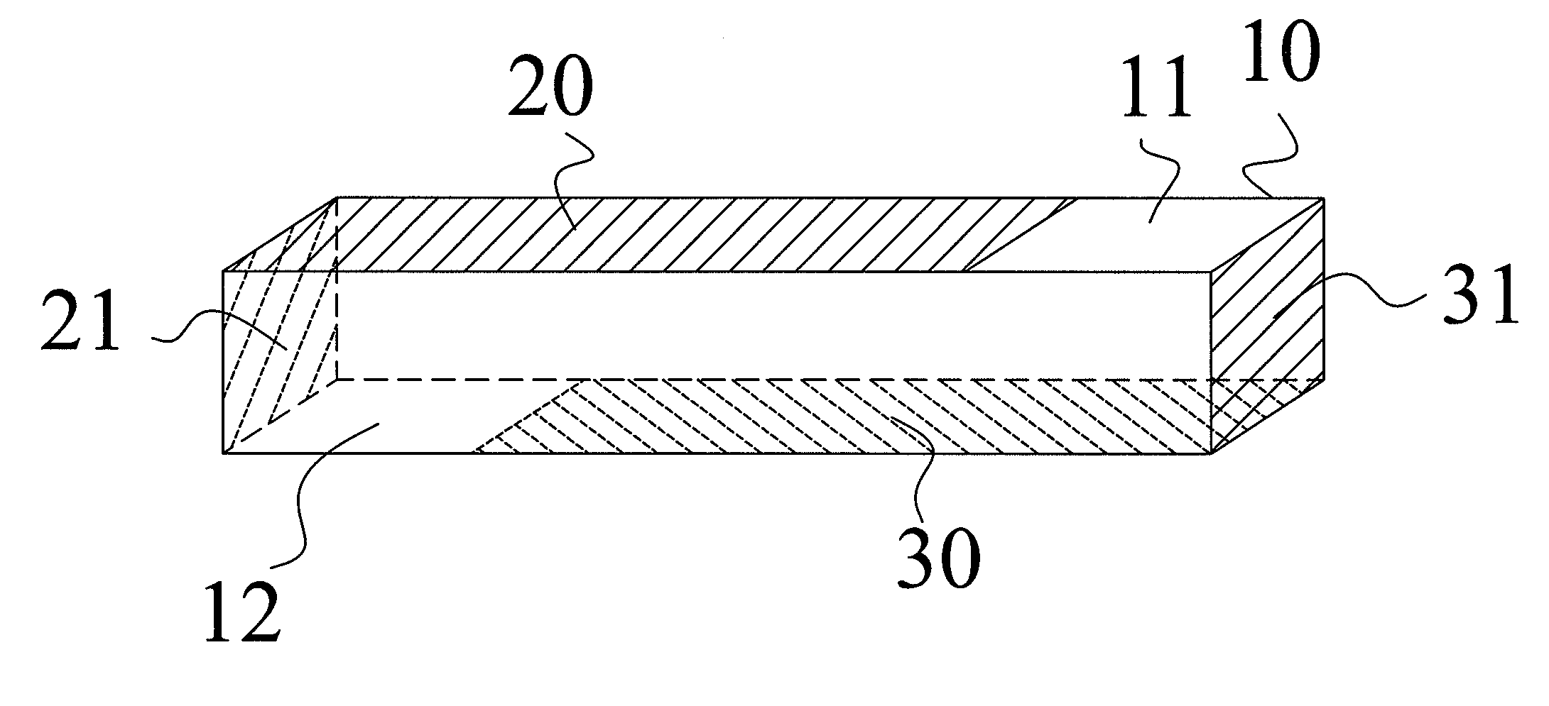
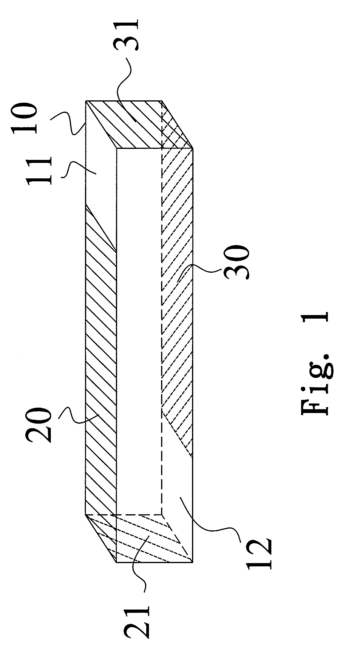
[0030]In the present invention, the resonant frequency can be easily adjusted via varying the capacitance of the antenna. In other words, the antenna can receive different frequencies via varying the shape and design of the antenna or via varying the dielectric constant of the dielectric element 10. Refer to FIG. 6 for the present invention. A portion of the first electrode layer 20 and a portion of the second electrode layer 30 are fabricated to have a serpentine shape, thereby increase the length of the first electrode layer 20 and the second electrode layer 30. Thus the receiving frequency of the antenna can be varied via varying the capacitance or the length of the electrodes of the antenna.
fourth embodiment
[0031]Based on the abovementioned principles and fabrication processes, arrays of antennae, as shown in FIG. 7 for the present invention can be mass-produced simultaneously on the carrier substrate 40. These arrays of antennae on carrier substrate 40 can be cut into individual miniature antenna with single operating frequency (similar to case shown in FIG. 5(d)). Alternatively, several miniature antennae, each having different operating frequency via varying its shape, design or dielectric element permittivity, can be fabricated on one carrier substrate 40. An integral antenna structure is thus formed which is suitable for devices that require multi-frequency signal transmitting / receiving capability (similar to case shown in FIG. 5(c)).
PUM
 Abstract
Description
Claims
Application Information
 - R&D
- Intellectual Property
- Life Sciences
- Materials
- Tech Scout
- Unparalleled Data Quality
- Higher Quality Content
- 60% Fewer Hallucinations
Browse by: Latest US Patents, China's latest patents, Technical Efficacy Thesaurus, Application Domain, Technology Topic, Popular Technical Reports.
© 2025 PatSnap. All rights reserved.Legal|Privacy policy|Modern Slavery Act Transparency Statement|Sitemap|About US| Contact US: help@patsnap.com


