
Method for patterning polycrystalline indium tin oxide

a technology of polycrystalline indium tin oxide and patterning method, which is applied in the direction of auxillary shaping apparatus, basic electric elements, manufacturing tools, etc., can solve the problems of low-temperature processing, defects in the layers below, and the substrate cannot stand temperatur

Inactive Publication Date: 2010-04-29
IND TECH RES INST
View PDF5 Cites 10 Cited by
  • Summary
  • Abstract
  • Description
  • Claims
  • Application Information

AI Technical Summary

Benefits of technology

[0009]The method for patterning polycrystalline indium tin oxide according to the present invention uses a focusing lens set to focus the Gaussian laser source and controls the laser parameters such as the energy profile, the pulse rate, the pulse repetition rate, the scanning speed and the light spot size to perform local

Problems solved by technology

However, plastic substrates cannot stand temperature over, for example, 300° C. Therefore, low-temperature processing is required.
However, convention laser machining results in thermal effects to cause elevated ridges on the edge and defects in the layers below.
However, such laser machining suffers from poor precision and thermal effects to cause elevated ridges on the edge and defects in the layers below.
Moreover, precision laser optic system for patterning fine line pitch is costly.
However, in this patent, thermal effects resulting from the long-pulse laser lead to poor patterning precision.
Moreover, a mask is needed and the patterning of fine line pitch is not available because the precision is limited by the optic diffraction limits.

Method used


Image

  • Method for patterning polycrystalline indium tin oxide
  • Method for patterning polycrystalline indium tin oxide
  • Method for patterning polycrystalline indium tin oxide

Examples


Embodiment Construction

[0022]The present invention can be exemplified but not limited by the embodiments as described hereinafter.

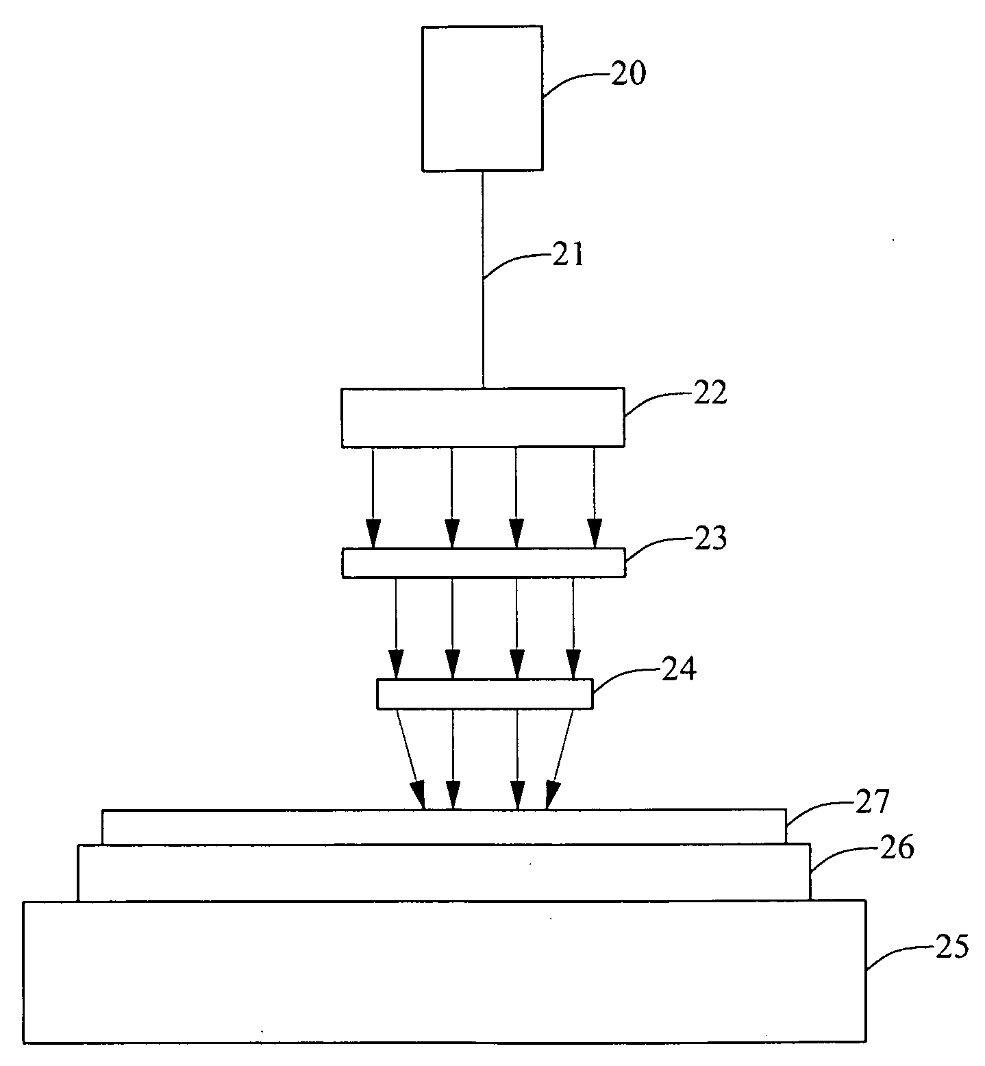
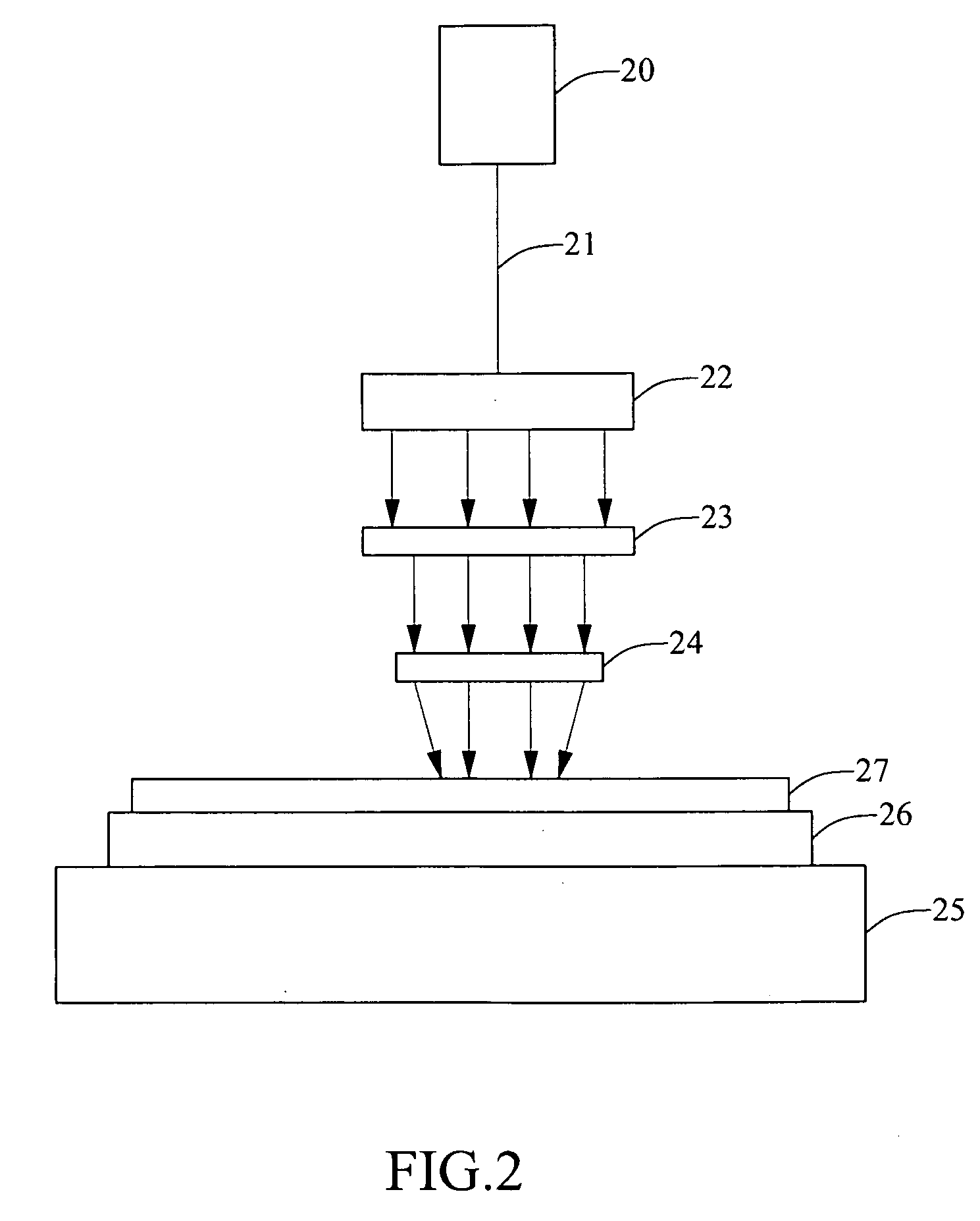
[0023]Please refer to FIG. 3, which is a system diagram for transferring amorphous ITO into polycrystalline ITO according to the present invention. The system comprises a laser source 30, a beam adjusting device 31, a focusing lens set 32 and a carrier 33. The laser source 30 is capable of generating a Gaussian laser beam 35. The beam adjusting device 31 is capable of adjusting the path and the energy intensity of the Gaussian laser beam 35. The focusing lens set 32 is capable of focusing the Gaussian laser beam 35. The carrier 33 is capable of moving relatively to the Gaussian laser beam 35 and carrying a substrate 36 with an amorphous ITO layer (not shown) formed thereon. To further monitor the system, the system further comprises an integrated control device 34 capable of monitoring the surface of the polycrystalline indium tin oxide layer to further optimize the process.

[00...


PUM

PropertyMeasurementUnit
Wavelengthaaaaaaaaaa
Energy intensityaaaaaaaaaa
Threshold limitaaaaaaaaaa

Abstract

A method for patterning polycrystalline indium tin oxide by using a Gaussian laser beam focused on an amorphous indium tin oxide layer is disclosed to pattern the non-crystalline amorphous indium tin oxide layer and transfer part of the amorphous indium tin oxide layer into polycrystalline indium tin oxide while the remaining amorphous indium tin oxide layer is etched due to etching selectivity of an etching solution. The method comprises: providing a substrate with an amorphous indium tin oxide layer thereon on a carrier; transferring the amorphous indium tin oxide layer in a predetermined area into a polycrystalline indium tin oxide layer by emitting a Gaussian laser beam focused on the amorphous indium tin oxide layer in the predetermined area; and removing the remaining amorphous indium tin oxide layer on the substrate by an etching solution to form a patterned polycrystalline indium tin oxide layer.

Description

BACKGROUND OF THE INVENTION[0001]1. Field of the Invention[0002]The present invention generally relates to a method for patterning polycrystalline indium tin oxide and, more particularly, to a method for patterning polycrystalline indium tin oxide by using a Gaussian laser beam focused on an amorphous indium tin oxide layer to pattern the non-crystalline amorphous indium tin oxide layer and transfer part of the amorphous indium tin oxide layer into polycrystalline indium tin oxide while the remaining amorphous indium tin oxide layer is etched due to etching selectivity of an etching solution.[0003]2. Description of the Prior Art[0004]In order to improve the device characteristic of the optoelectronic products such as solar cells and flat-panel displays, the amorphous material such as the transparent conductive oxide has to be transferred by thermal treatment into polycrystalline material so as to reduce the resistivity and enhance the transparency. Recently, flexible plastic substra...

Claims


Application Information

Patent Timeline
IPC IPC(8): H01L21/20B29B13/08
CPCH01L21/02565H01L21/02678Y02E10/50H01L31/1884H01L31/022466H01L31/022475
Inventor CHENG, CHUNG-WEICHEN, HWEI-SHENCHEN, JENQ-SHYONG
Owner IND TECH RES INST
Learn More