
Nanostructured titania

a nanostructured titania and nano-structure technology, applied in the direction of solid-state diffusion coating, instruments, transportation and packaging, etc., can solve the problems of poor yield, lowering process yield, and other methods used with this method are not compatible with high-volume semiconductor manufacturing processes, so as to achieve high edge acuity and better edge acuity

Active Publication Date: 2010-04-08
RGT UNIV OF CALIFORNIA
View PDF6 Cites 1 Cited by
  • Summary
  • Abstract
  • Description
  • Claims
  • Application Information

AI Technical Summary

Benefits of technology

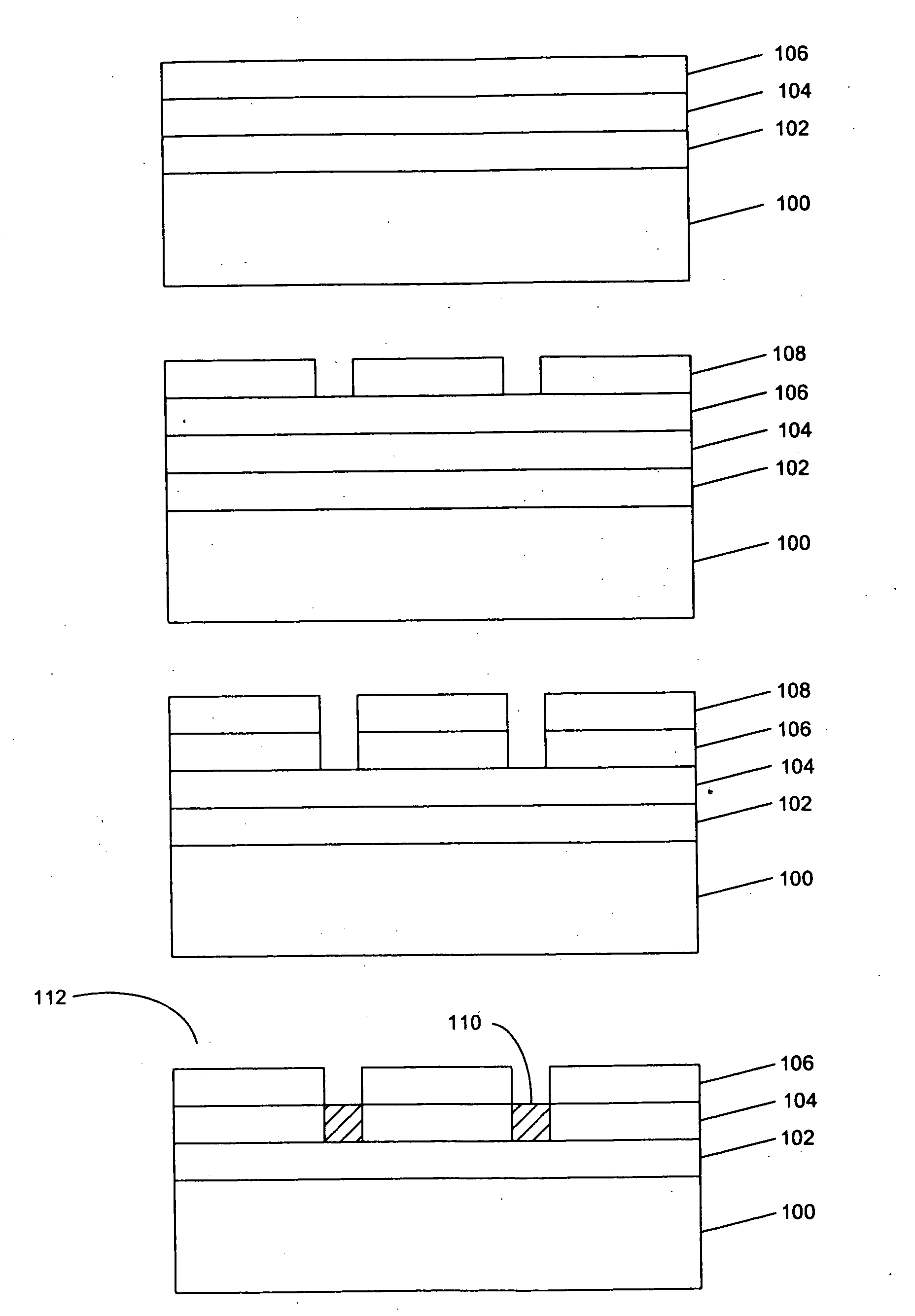
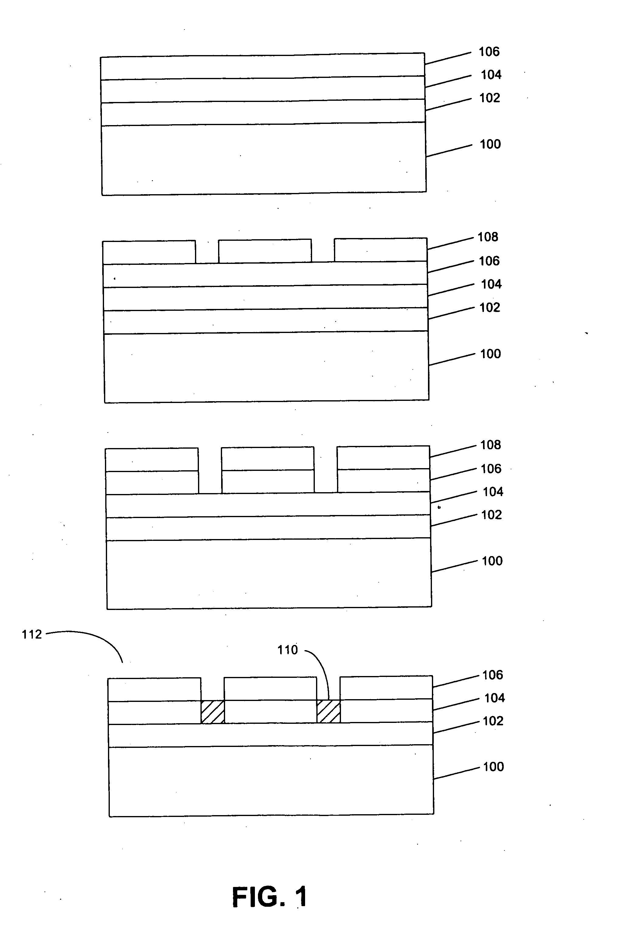
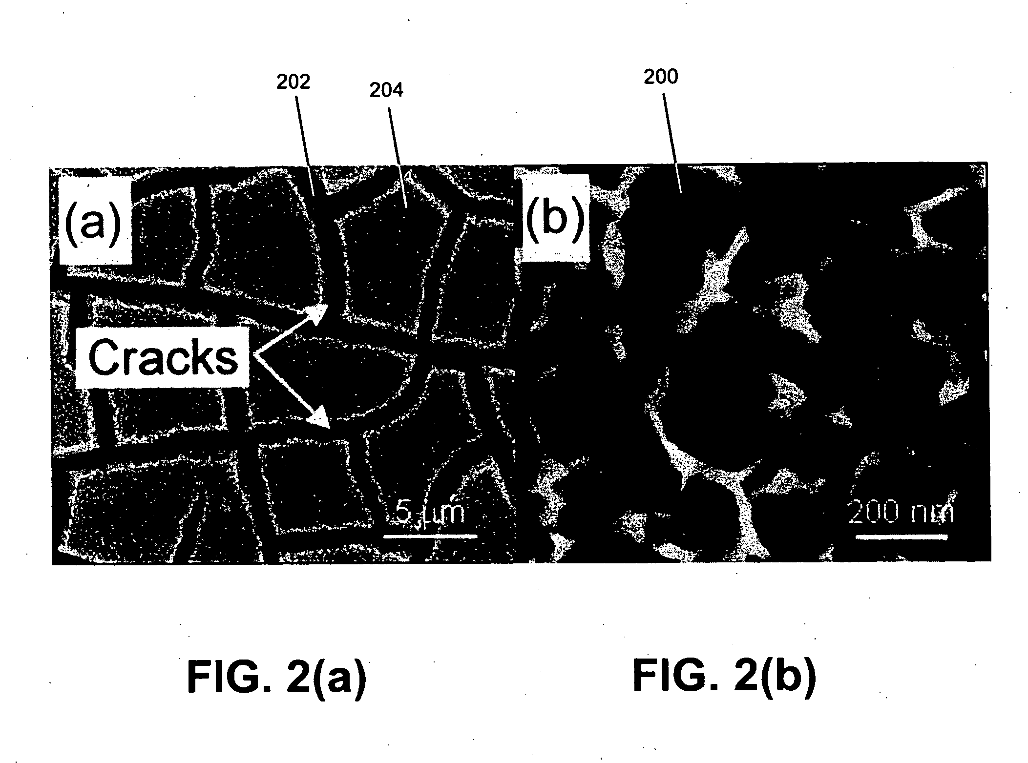
[0016]The issues of crack formation in TiO2 and delamination of TiO2 features from the underlying substrate can, however, be eliminated by oxidizing exposed surfaces of Ti thin films that have been masked to below a threshold area. For example by reacting patterned Ti films of 20 mm squares with hydrogen peroxide, cracks can be eliminated in TiO2 features formed. In addition, TiO2 features thus formed have better edge acuity than those formed using the SAMs technique. Furthermore, the issue of carbon incorporation does not arise since high purity Ti film is used instead of organic precursors. In addition, the technique disclosed uses process tools and material sets that are already in use in the semiconductor industry. Hence the technique is compatible with current manufacturing processes.
[0017]It is the object of the invention described in this disclosure to provide a method of forming, on an electronic component, patterned NST elements that are crack free, have high edge acuity and with sizes from about 300 micrometers or less. In another aspect, this disclosure provides a method of constructing a chemical sensing element, comprising providing patterned NST features, fabricated using the aforementioned process, on an electronic circuit and depositing electrodes on the NST features. In a further aspect, this disclosure provides a method of constructing patterned nanocomposites comprised of metal and NST features fabricated using the aforementioned process, suitable for use as wear resistant electrical contacts on electronic components. In still another aspect of the invention, the NST elements fabricated in accordance with the foregoing process are porous and have pores of various selectable diameters. The elements of the invention can be incorporated in microcircuits and are biocompatible.

Problems solved by technology

It is noted that except reactive ion etching, other techniques used with this method are not compatible with high-volume semiconductor manufacturing processes.
Also the probability of adjacent paste developing bridges increases as the pitch decreases, thus lowering process yield.
Because surface coverage of SAM is, in most cases, not high, this method results in poor yield especially when large-area substrates are used.
In addition, relatively long time—up to a few hours—is required for deposition of TiO2 using this method.
In addition, edge acuity, or the ratio of standard deviation to the mean of a sample of pattern widths, of titania features formed using this technique is relatively poor, namely, about 2.1% in the state of the art.
This latter problem makes it extremely difficult to use this method to form submicrometer features with very small separation.
It is, therefore, becoming increasingly difficult to form miniaturized features of porous TiO2 in integrated circuitry.
However, in all these cases, titania layers formed by reacting aqueous hydrogen peroxide have high crack density and delaminated extensively from the underlying substrate making them unsuitable for applications in integrated microelectronic circuits.

Method used


Image

  • Nanostructured titania
  • Nanostructured titania
  • Nanostructured titania

Examples


Embodiment Construction

[0032]In the following description, reference is made to the accompanying drawings which form a part hereof, and which is shown, by way of illustration, several embodiments of the present invention. It is understood that other embodiments may be utilized and structural changes may be made without departing from the scope of the present invention.

Overview and Related Publications Incorporated by Reference

[0033]The present invention relates to formation of nanostructured titania (NST) from patterned Ti films. To prove the effectiveness of patterning to reduce and eliminate crack formation, NST was also formed on blanket (unpatterned) Ti films.

[0034]Additional description of the process for fabricating crack fee nanostructured titania (NST, or ns-titania) is found in Appendices A-H of provisional patent application Ser. No. 60 / 667,667, the disclosure and appendices of which are an integral part of this application and which are also hereby incorporated herein by reference.

Experimental ...


PUM

PropertyMeasurementUnit
diameteraaaaaaaaaa
sizesaaaaaaaaaa
pressureaaaaaaaaaa

Abstract

A method and device of nanostructured titania that is crack free. A method in accordance with the present invention comprises depositing a Ti film on a surface, depositing a masking layer on the Ti film, etching said masking layer to expose a limited region of the Ti film, the limited region being of an area less than a threshold area, oxidizing the exposed limited region of the Th.ucsbi film, and annealing the exposed limited region of the Ti film.

Description

CROSS-REFERENCE TO RELATED APPLICATIONS[0001]This application claims the benefit under 35 U.S.C. Section 119(e) of co-pending and commonly-assigned U.S. provisional patent application Ser. No. 60 / 667,667, filed Apr. 4, 2005, entitled “NANOSTRUCTURED TITANIA,” by Zuruzi A. Samah et al., which application is incorporated by reference herein.BACKGROUND OF THE INVENTION[0002]1. Field of the Invention[0003]The present invention relates generally to a method of forming patterned nanostructured titania (NST) features, and in particular for forming NST features for various electronic applications such as chemical sensing, wear-resistant electrical contacts and photovoltaics.[0004]2. Description of the Related Art[0005]Patterned nanoporous titania (NST) thin films are well known in many prior reports. For instance, NST has been used in chemical detection systems, catalysis and solar energy conversion. In one widely used conventional method (called the sol-gel method), patterned features of T...

Claims


Application Information

Patent Timeline
Patent Type & Authority Applications(United States)
IPC IPC(8): B32B3/10C23C16/40
CPCG01N27/125Y10S977/89Y10S977/888Y10T428/24331Y10S977/781Y10S977/784Y10S977/811
Inventor SAMAH, ZURUZI ABUMACDONALD, NOEL C.WARD, MARCUSMOSKOVITS, MARTINKOLMAKOV, ANDREISAFINYA, CYRUS R.
Owner RGT UNIV OF CALIFORNIA
Learn More