Semiconductor memory device

Inactive Publication Date: 2010-04-01
SEMICON ENERGY LAB CO LTD
View PDF21 Cites 36 Cited by
  • Summary
  • Abstract
  • Description
  • Claims
  • Application Information

AI Technical Summary

Benefits of technology

[0007]However, since detecting addresses of a defective memory cell and an unused spare memory is needed to correct a defect, the number of access to a memory is increased with an increase of a memory capacity and it makes time for access to the memory longer. Further, a structure of a control circuit is enlarged with an increase of the memory capacity.
[0008]In view of the above problems, it is an object to realize easy and fast access to a memory without enlargement of a structure of a control circuit.
[0015]In the semiconductor memory device, an address of a defective memory cell is judged in accordance with the number of correcting defects. Therefore, easier and faster operation can be realized. In addition, the operation can be applied to a high-capacity memory.

Problems solved by technology

However, since detecting addresses of a defective memory cell and an unused spare memory is needed to correct a defect, the number of access to a memory is increased with an increase of a memory capacity and it makes time for access to the memory longer.

Method used


Image

  • Semiconductor memory device
  • Semiconductor memory device
  • Semiconductor memory device

Examples


embodiment 1

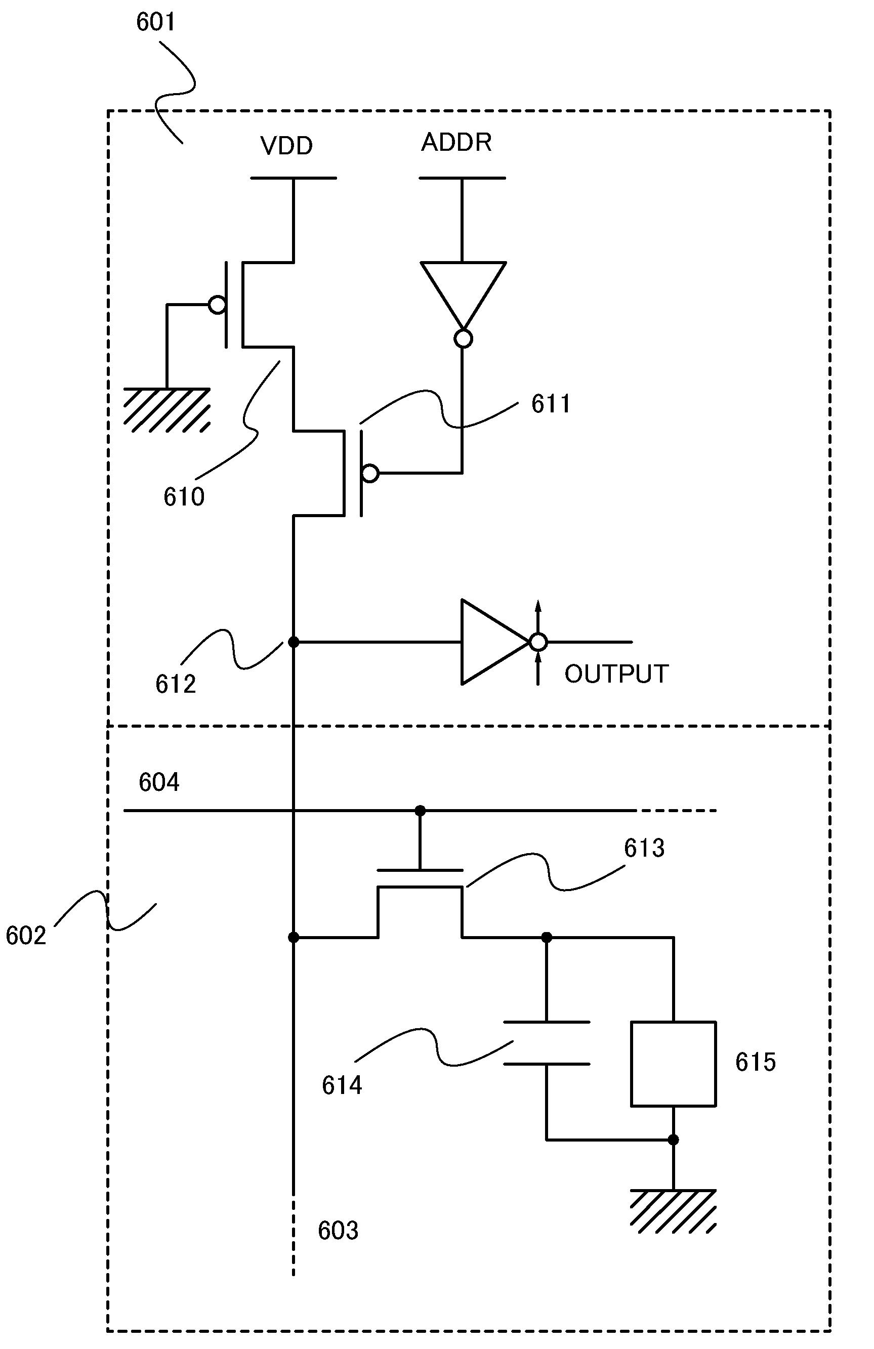
[0032]In this embodiment, an example of a semiconductor memory device and a technology for correcting defects in the semiconductor memory device will be described.

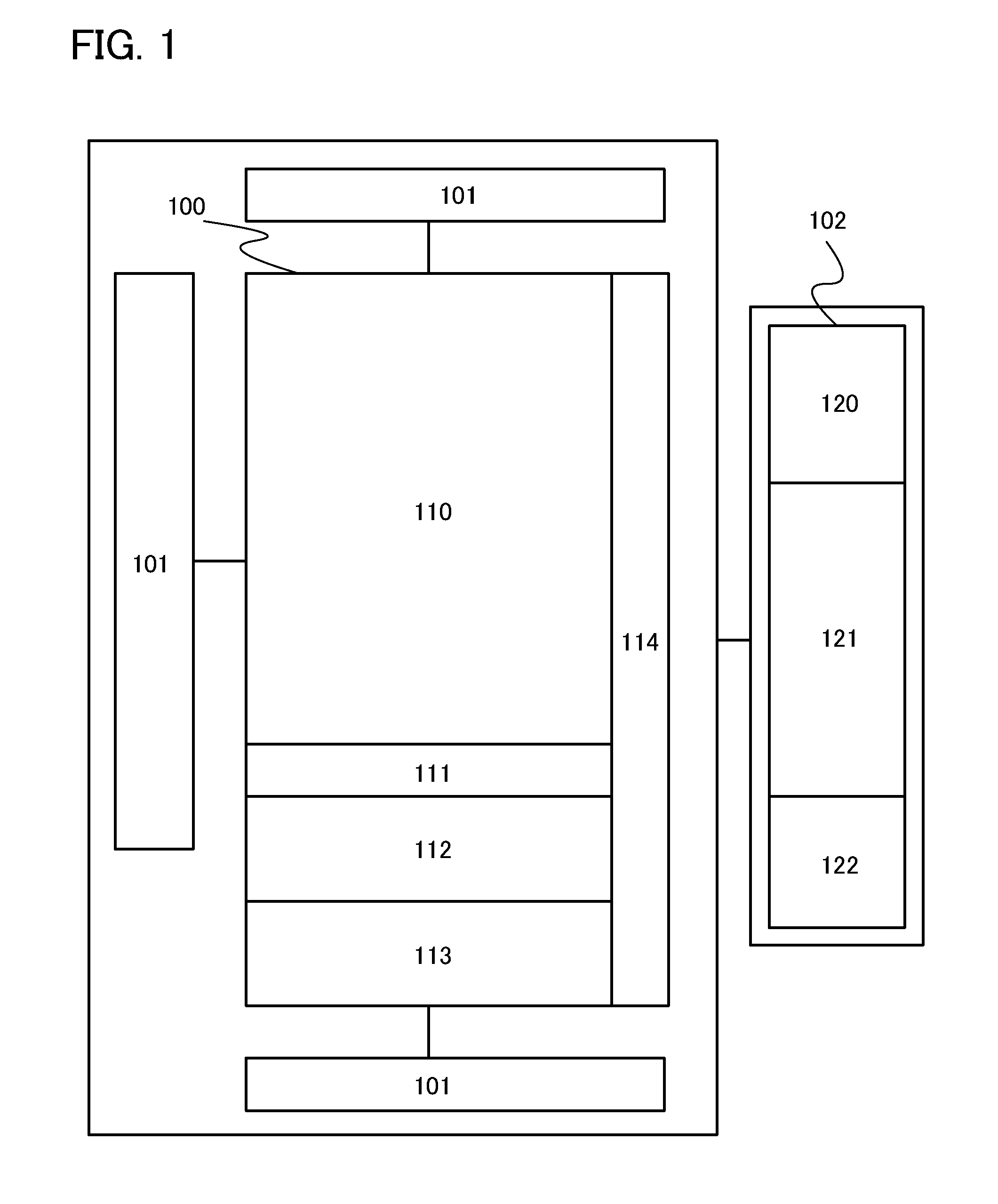
[0033]First, an example of a structure of a semiconductor memory device will be described with reference to FIG. 1. Here, FIG. 1 is a circuit block diagram of the semiconductor memory device according to this embodiment. As shown in FIG. 1, the semiconductor memory device includes a memory cell array 100, and a reading driver 101 and a redundant control circuit portion 102 which are around the main memory cell array 100.

[0034]The memory cell array 100 includes a main memory cell 110, a spare memory cell, and a memory cell 114 for preventing additional writing. Note that the spare memory cell is provided with a memory cell 111 for a redundant function, a memory cell 112 for redundant judgment, and a memory cell 113 for replacement.

[0035]Input data is written in the main memory cell 110 and the memory cell 113 for replacemen...

embodiment 2

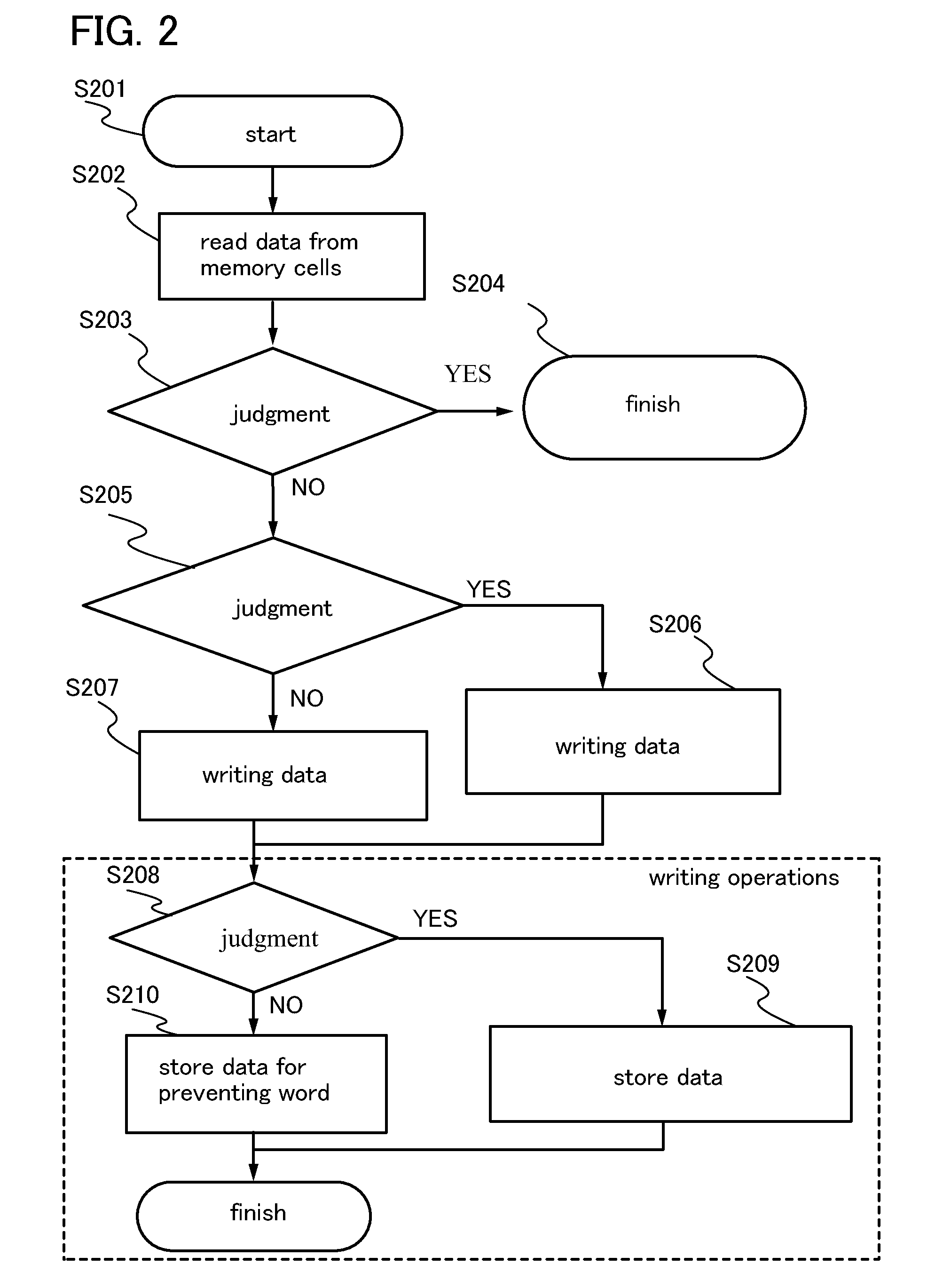
[0124]In this embodiment, an example of a method of writing data to memory cells in the semiconductor memory device is described.

[0125]In this semiconductor memory device, operation A, operation B, and operation C are alternately executed at most 4 times when data is written to a memory cell: operation A; data is written during a predetermined period (for example, 75.5 μs), operation B; data is read during a predetermined period (for example, 18.9 μs), and operation C; the written data and the read data are compared. Note that hereinafter the data comparison according to operation C is referred to as “verify function,” a series of operations A, B, and C is referred to “verify writing.”

[0126]If the results of the verify function do not match each other when the verify writing is repeated 4 times to one memory cell, the data α that the result do not match is kept inside a circuit as information and after that the process proceeds to the next memory cell. On the other hand, if the resu...

embodiment 3

[0131]In this embodiment, an example of a structure of a semiconductor device capable of wireless communication is described with reference to FIG. 11. Here, FIG. 11 is a circuit block diagram showing a semiconductor device 900 capable of wireless communication. As shown in FIG. 11, the semiconductor device 900 includes a memory circuit 901, a digital circuit 902, an analog circuit 903, and an antenna circuit 904.

[0132]The antenna circuit 904 receives a radio wave (an electromagnetic wave) transmitted from a reader / writer 910 and inputs a signal obtained at that time to the analog circuit 903. The analog circuit 903 demodulates a signal and inputs a demodulated signal to the digital circuit 902. The memory circuit 901 executes writing or reading of data in response to an output from the digital circuit 902.

[0133]By applying the semiconductor memory device according to the present invention to the memory circuit 901, a highly reliable semiconductor device which can operate fast can b...


PUM


Abstract

Easy and fast memory access with correcting defects is to be realized. In a spare memory in a semiconductor memory device, a redundant memory cell array that stores the number of correcting defects is provided. When a signal from the outside is received, the signal is switched to the redundant memory cell array, and the number of correcting defects is judged. Then, based on the result of the judgment, it is determined the judgment of a defective memory cell is continued or the judgment is finished to write data to a main memory cell. By providing the redundant memory cell array that stores the number of correcting defects, a state of correcting defects can be observed fast in such a manner.

Description

TECHNICAL FIELD[0001]The technical field relates to a defect correcting technology in a semiconductor memory device.BACKGROUND ART[0002]In recent years, the yield of memory cells tends to decrease due to an increase and a complexity of manufacturing steps with an increase in the capacity of a semiconductor memory device. Thus, various kinds of a defect correcting technology for a memory cell array including a defective memory cell in order to improve the yield of a semiconductor memory device itself has been suggested.[0003]For example, a technology for correcting a defect, by replacing a memory cell which is determined to be defective by a redundant circuit provided in the semiconductor memory device with a spare cell has been suggested (for example, see Patent Document 1).[0004]In addition, a technology for correcting a defect by replacing a defect generated in a DRAM (dynamic random access memory) in a semiconductor memory device with a RAM portion for redundancy in a LSI for cor...

Claims


Application Information

Patent Timeline
IPC IPC(8): G11C29/00
CPCG11C16/3459G11C16/349G11C29/44G11C2029/4402G11C29/808G11C2029/0409G11C2029/0411G11C29/4401
Inventor OHMARU, TAKUROATSUMI, TOMOAKISAITO, TOSHIHIKO
Owner SEMICON ENERGY LAB CO LTD
Why Eureka
Try Eureka