Infra-red light stimulated high-flux semiconductor x-ray and gamma-ray radiation detector

a high-flux semiconductor and detector technology, applied in the field of detection radiation, can solve the problems of space-charge formation, space-charge formation and potential temporary paralysis of the device called polarization, and the breakage of the energy peak, so as to achieve the effect of dramatically reducing the residence time of the charge carrier

Inactive Publication Date: 2010-04-01
PRODUCE
View PDF5 Cites 31 Cited by
  • Summary
  • Abstract
  • Description
  • Claims
  • Application Information

AI Technical Summary

Benefits of technology

[0014]The present invention is a method by which the residence time of charge carriers is dramatically reduced by an external optical energy source and the occupancy of the deep level defects is maintained close to the thermal equilibrium of the un-irradiated device even under high-flux expos

Problems solved by technology

Fluctuation in the pulse amplitude due to electronic noise results in a broadening of the energy peak, while charge loss in the detector due to trapping or recombination results in reduced pulse amplitude and a low energy tail in the energy peak.
First, under high-flux operating conditions such as in medical, security and industrial Computed Tomography, photon fluxes in many millions of photons per second per square millimeter are used.
Under such conditions, hole trapp

Method used


Image

  • Infra-red light stimulated high-flux semiconductor x-ray and gamma-ray radiation detector
  • Infra-red light stimulated high-flux semiconductor x-ray and gamma-ray radiation detector
  • Infra-red light stimulated high-flux semiconductor x-ray and gamma-ray radiation detector

Examples


Embodiment Construction

[0029]The present invention is described with reference to the accompanying figures where like reference numbers correspond to like elements.

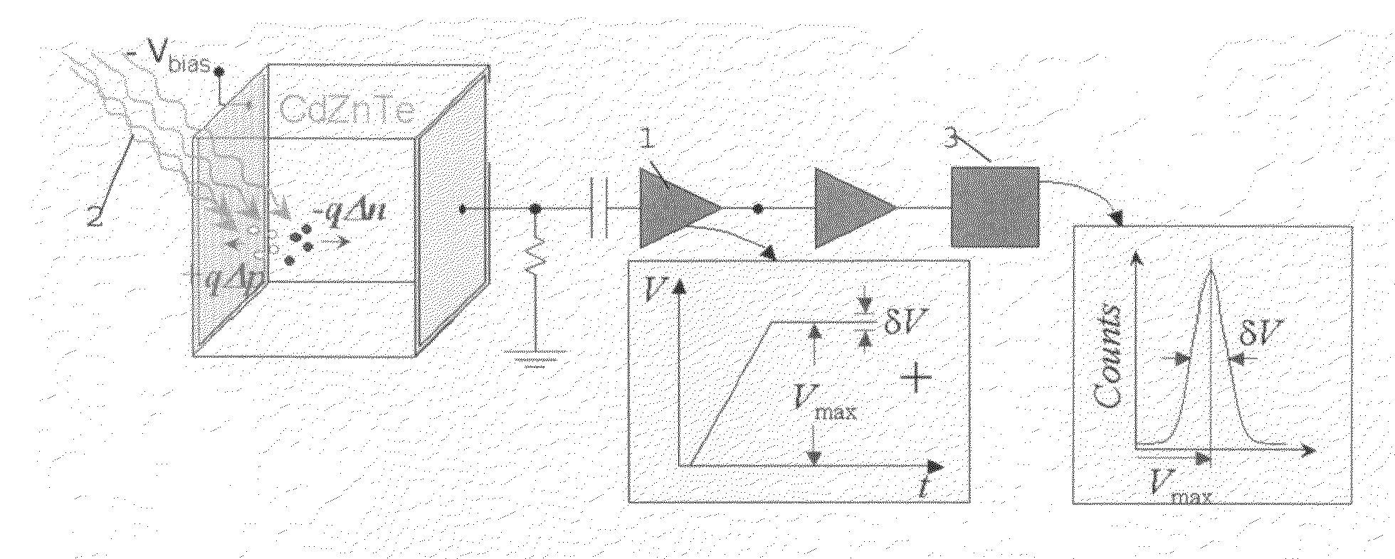
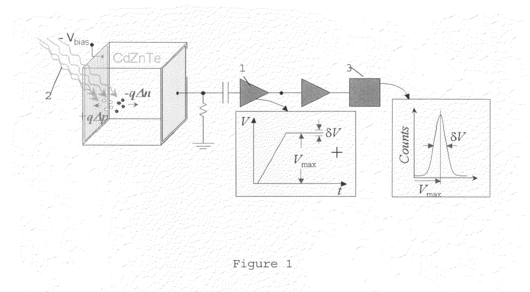
[0030]The operation principle of typical pulse-mode semiconductor detectors is shown in FIG. 1. Current is typically integrated by a charge sensitive preamplifier 1 to measure the total charge induced by the outside radiation 3 and produces a voltage pulse (not shown) with amplitude proportional to the total induced charge. Photons with various energies produce voltage pulses in the preamplifier 1 with various amplitude and individual peaks with various peak positions in the multi-channel analyzer 3. Fluctuation in the pulse amplitude due to electronic noise results in a broadening of the energy peak, while charge loss in the detector due to trapping or recombination results in reduced pulse amplitude and a low energy tail in the energy peak.

[0031]FIG. 2 illustrates the situation when high-speed, high-flux x-ray applications, such as diagnostic...


PUM


Abstract

A method of detecting radiation through which the residence time of charge carriers is dramatically reduced by an external optical energy source and the occupancy of the deep-level defects is maintained close to the thermal equilibrium of the un-irradiated device even under high-flux exposure conditions. Instead of relying on thermal energy to release the trapped carriers, infra-red light radiation is used to provide sufficient energy for the trapped carriers to escape from defect levels. Cd1-xZnxTe crystals are transparent to infra-red light of this energy and no additional absorption occurs other than the one associated with the ionization of the targeted deep-level defects. This allows irradiation geometry from the side source of the Cd1-xZnxTe detector crystals.

Description

RELATED APPLICATION[0001]The present patent application is a continuation-in-part of U.S. provisional patent application Ser. No. 61 / 100,358, filed Sep. 26, 2008, hereby incorporated, and claims the priority date thereof.FIELD OF INVENTION[0002]The present invention relates to detecting radiation and, more specifically, to a method by which infra-red light radiation is used to provide sufficient energy for trapped charge carriers to escape from defects levels.BACKGROUND OF THE INVENTION[0003]Historically, semi-insulating Cd1-xZnxTe crystals (where 0≦x<1) with Zn composition in the 0≦x≦0.25 mole fraction range are typically used for room-temperature semiconductor radiation detector applications. In order to be useful for x-ray and gamma-ray detectors the Cd1-xZnxTe crystals must be electrically compensated to bring them to a highly resistive state so that the equilibrium residual free carrier concentration is much lower than that of the free carriers generated by the impinging x-r...

Claims


Application Information

Patent Timeline
IPC IPC(8): G01T7/00G01T1/00G01T1/24
CPCG01T1/00G01T1/24
Inventor SZELES, CSABAPROKESCH, MICHAELBALE, DEREKGLICK, BRUCECRAWFORD, CARL
Owner PRODUCE
Why Eureka
Try Eureka