
Printed Circuit Board for Harsh Environments

a technology of printed circuit boards and harsh environments, which is applied in the manufacture of final products, electrical apparatus construction details, sustainable manufacturing/processing, etc., can solve the problems of not working in the range of thousands of g, the device attached to the circuit board is also stressed, and the high temperature environment of a gas turbine exceeds the temperature capability of polymeric encapsulating materials such as silicon gel or epoxy materials

Active Publication Date: 2010-04-01
SIEMENS ENERGY INC +1
View PDF54 Cites 15 Cited by
  • Summary
  • Abstract
  • Description
  • Claims
  • Application Information

AI Technical Summary

Benefits of technology

[0004]One exemplary prior art device is disclosed in U.S. Pat. No. 5,081,562, entitled CIRCUIT BOARD WITH HIGH HEAT DISSIPATIONS CHARACTERISTIC. This patent teaches fabrication of a circuit board having a cavity for receiving an integrated circuit device and connecting leads from circuit traces on the top rim of the cavity to connection pads on the IC. This arrangement allows the connecting leads to lie flat. However, the attachment of the device to the circuit board is also stressed significantly when the PCB is exposed to centrifugal forces in the thousands of Gs. There is no suggestion or teaching of a structure that can withstand high G-forces

Problems solved by technology

However, the attachment of the device to the circuit board is also stressed significantly when the PCB is exposed to centrifugal forces in the thousands of Gs.
This arrangement ensures structural integrity during vibration and G-forces in the range of 10 G's but would not work in the range of thousands of G's.
Moreover, the high temperature environment of a gas turbine exceeds the temperature capability of polymeric encapsulating materials, such as silicon gel or epoxy materials.

Method used


Image

  • Printed Circuit Board for Harsh Environments
  • Printed Circuit Board for Harsh Environments
  • Printed Circuit Board for Harsh Environments

Examples


Embodiment Construction

[0015]The inventors have recognized that the prior art PCB's are inadequate for the harsh environment of a gas turbine, and in particular are inadequate for the high G-forces of a turbine blade to which the PCB is attached. Applicants also have recognized that a better geometry is needed to support circuit components when subjected to extremely high G-forces.

[0016]The components of the circuitry supported by the PCB disclosed herein enable transmission of data via wireless telemetry circuits from regions of a gas turbine with temperatures ranging from ambient to greater than 350° C., and may include temperatures up to at least 450° C. This type of design strategy must be useful for incorporating instrumentation on a rotating hot section component, such as a gas turbine blade being subjected to G-forces in excess of 1,000 G's, because the PCB must be located on the turbine blade, and thus operate at temperatures exceeding 450° C.

[0017]One such instrumented moving hot section componen...


PUM


Abstract

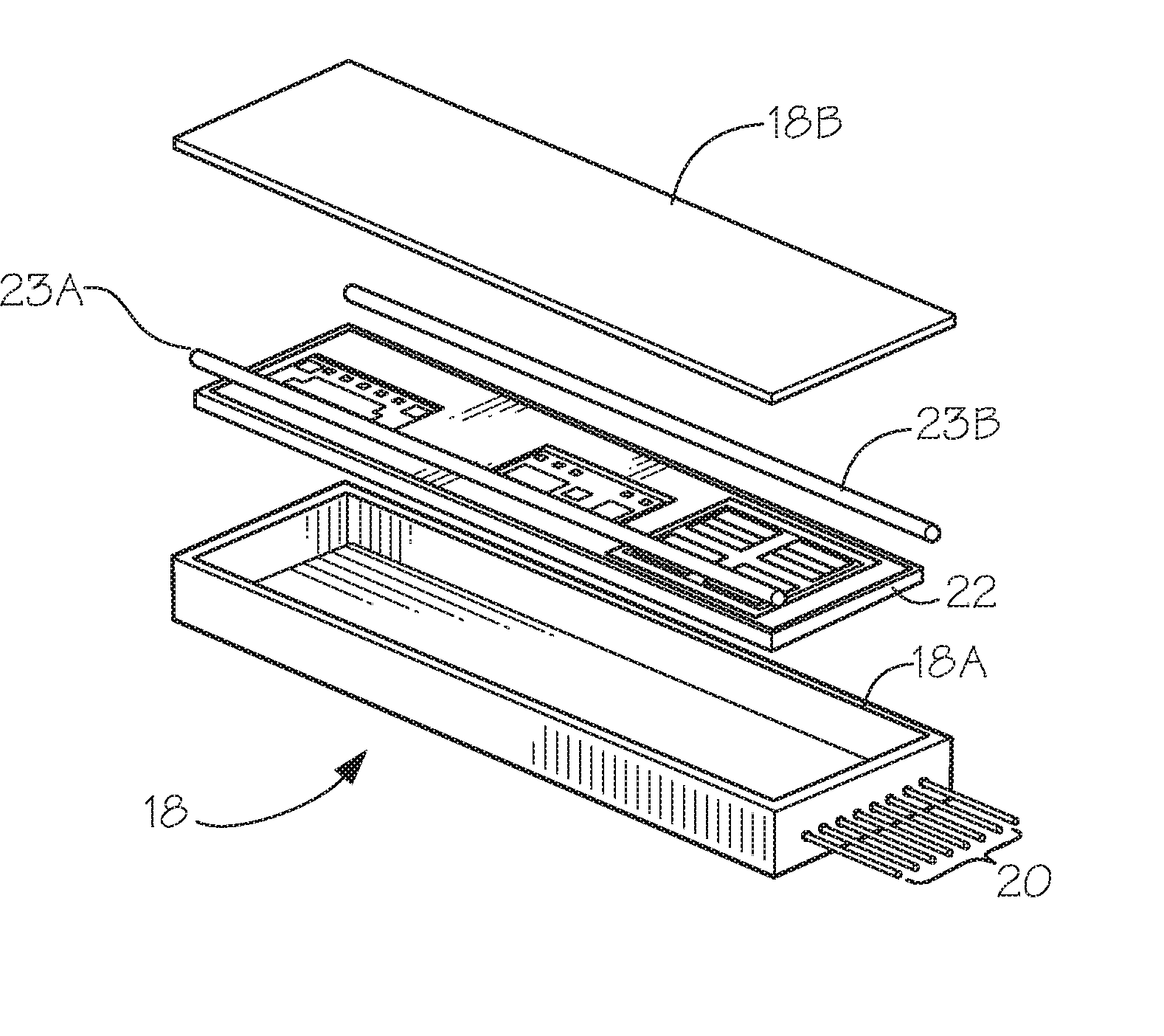
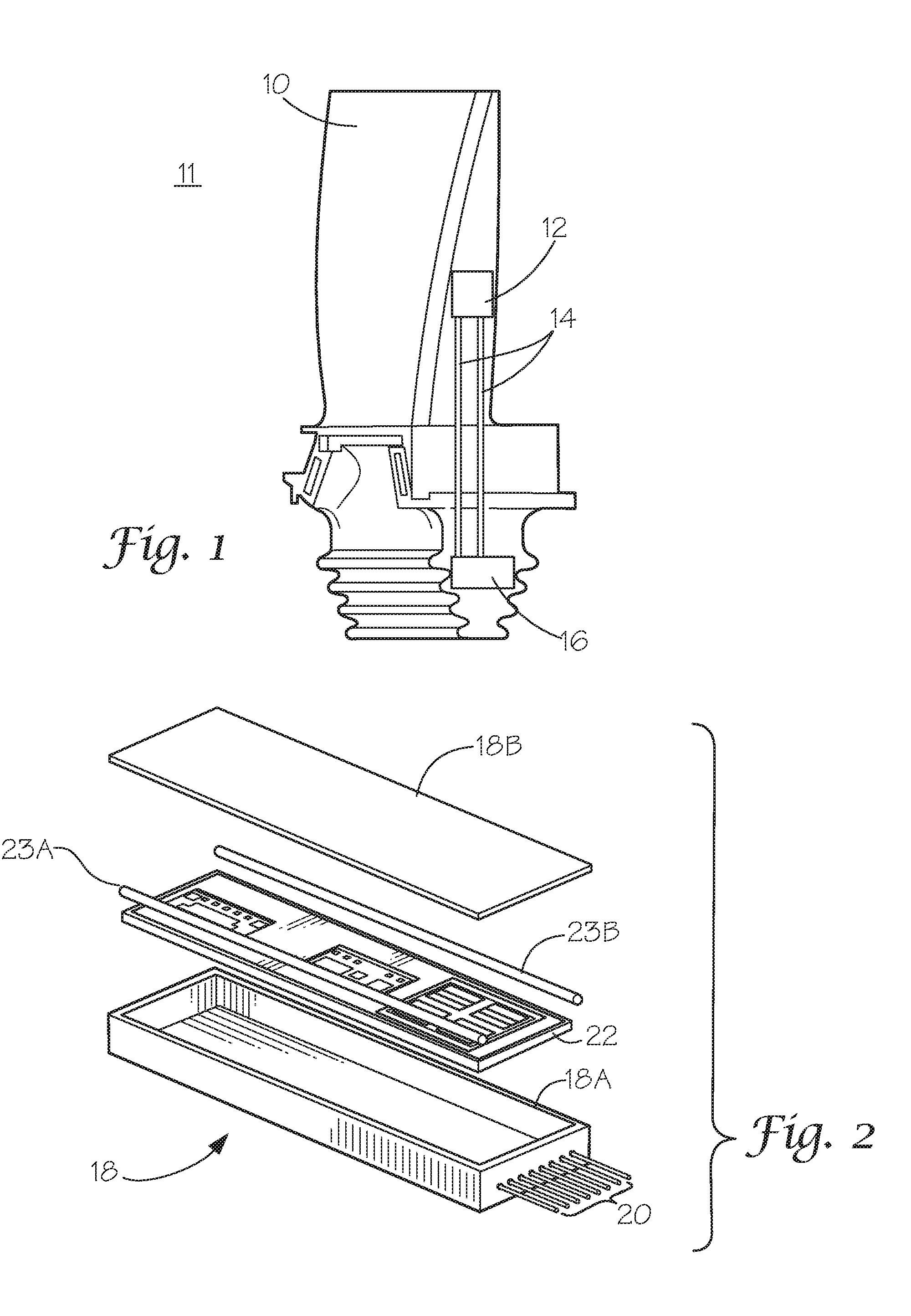
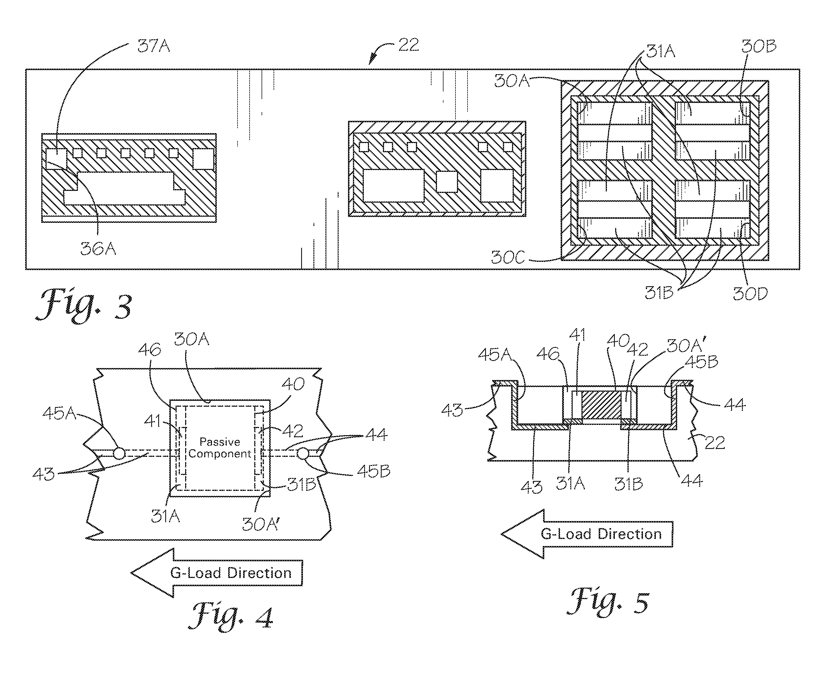
A printed circuit board (PCB 22) capable of withstanding ultra high G forces and ultra high temperature as in a gas turbine (11). The PCB includes a substrate having a plurality of cavities (30A, 36A) formed therein for receiving components of a circuit, and conductors embedded in the PCB for electrically connecting the components together to complete the circuit. Each of the cavities has a wall (36A′) upstream of the G-forces which supports the respective component in direct contact in order to prevent the development of tensile loads in a bonding layer (37A). When the component is an integrated circuit (50), titanium conductors (63) are coupled between exposed ends of the embedded conductors and contact pads on the integrated circuit. A gold paste (51) may be inserted into interstitial gaps between the integrated circuit and the upstream wall.

Description

[0001]This application claims benefit of the 26 Sep. 2008 filing date of U.S. provisional application No. 61 / 100,442.FIELD OF THE INVENTION[0002]The present invention generally relates to printed circuit boards (PCB) and in particular to a PCB structure designed to withstand the harsh environment of ultra high G-forces and ultra high temperature, such as occur on the rotating hot gas path components of a gas turbine engine.BACKGROUND OF THE INVENTION[0003]The temperatures inside an operating gas turbine engine are extremely high, often at levels in excess of 350° C. When it is desirable to monitor the inside temperatures of components of the turbine, such as a rotating turbine blade being exposed to thousands of G's, or to monitor stresses placed upon such components during operation, a special sensing, amplifying and transmitting circuit is required. An effective solution to this problem is the use of wireless telemetry, such as that disclosed in published U.S. Patent Application P...

Claims


Application Information

Patent Timeline
IPC IPC(8): H05K1/00
CPCH01L24/28H01L2924/13062H01L24/48H01L24/83H01L24/85H01L2224/29344H01L2224/45014H01L2224/45144H01L2224/45164H01L2224/45166H01L2224/45181H01L2224/45184H01L2224/4554H01L2224/45669H01L2224/45684H01L2224/48091H01L2224/48472H01L2224/73265H01L2224/83801H01L2224/85205H01L2924/01012H01L2924/01014H01L2924/01046H01L2924/01078H01L2924/01079H01L2924/14H01L2924/15153H01L2924/15165H01L2924/19041H05K1/0271H05K1/0306H05K1/092H05K1/183H05K2201/10636H05K2201/10674H05K2203/049H01L24/45H01L2924/01028H01L2924/01013H01L2224/32225H01L2224/48227H01L2924/00013H01L2924/00014H01L2924/00H01L2924/3512H01L2224/29099H01L2224/05553H01L2224/29294H01L2224/85207H01L2924/00011H01L2924/10161Y02P70/50H01L2224/83205H01L2924/206H01L21/48H05K3/00H05K7/00
Inventor MITCHELL, DAVID J.KULKARNI, ANAND A.BURNS, ANDREW J.
Owner SIEMENS ENERGY INC
Learn More