Production method of metal oxide precursor layer, production method of metal oxide layer, and electronic device
a production method and metal oxide technology, applied in the direction of semiconductors, nuclear engineering, transportation and packaging, etc., can solve the problems of poor energy efficiency of thermal oxidation, difficult to achieve desired performance, and difficulty in application to resin substrates that are lightweight with flexibility, etc., to achieve excellent film forming properties, high on/off ratio, and enhanced mobility
- Summary
- Abstract
- Description
- Claims
- Application Information
AI Technical Summary
Benefits of technology
Problems solved by technology
Method used
Image
Examples
example 1
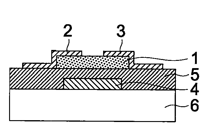
[0145]In FIG. 3, a production process of a thin film transistor is shown as a schematic cross-sectional view.
[0146]>
[0147]As substrate 6, a glass substrate was used and an ITO coated film of a thickness of 300 nm was formed entirely thereon. Thereafter, gate electrode 4 was formed by etching using a photolithographic method.
[0148]Subsequently, via an atmospheric pressure plasma method, gate insulation film 5 of a thickness of 200 nm composed of silicon oxide was formed. Herein, as an atmospheric pressure plasma apparatus, an apparatus based on FIG. 6 described in JP-A No. 2003-303520 was employed.
[0149](Gases Used)
[0150]Inert gas: 98.25% by volume of helium
[0151]Reactive gas: 1.5% by volume of oxygen gas
[0152]Reactive gas: 0.25% by volume of tetraethoxysilane vapor (bubbled with helium)
[0153](Discharge Conditions)
[0154]High frequency power supply: 13.56 MHz
[0155]Discharge power: 10 W / cm2
[0156](Electrode Conditions)
[0157]An electrode was produced by the following method. A stainless...
example 2
[0191]14-16>>
[0192]Thin film transistors 14-16 were produced in the same manner as in production of thin film transistor 3 of Example 1 except that temperature after film formation was adjusted at 100%, 150%, and 200%, respectively, of the boiling point of the main solvent (boiling point of water: 100° C.).
[0193]17-19>>
[0194]Thin film transistors 17-19 were produced in the same manner as in production of thin film transistor 10 of Example 1 except that temperature after film formation was adjusted at 98% (80° C.), 185% (150° C.), and 247% (200° C.), respectively, of the boiling point of acetonitrile (boiling point: 81° C.).
[0195]Film quality of metal oxide precursor layer 1a in the production process of obtained thin film transistors 14-19 each was observed using a microscope in the same manner as in film forming properties evaluation described in Example 1 and evaluated by ranking as described below.
[0196]A: A uniform thin film is formed and no defects such as cracks or fissures ar...
PUM
| Property | Measurement | Unit |
|---|---|---|
| temperature | aaaaa | aaaaa |
| temperature | aaaaa | aaaaa |
| forming temperature | aaaaa | aaaaa |
Abstract
Description
Claims
Application Information
 - R&D Engineer
- R&D Manager
- IP Professional
- Industry Leading Data Capabilities
- Powerful AI technology
- Patent DNA Extraction
Browse by: Latest US Patents, China's latest patents, Technical Efficacy Thesaurus, Application Domain, Technology Topic, Popular Technical Reports.
© 2024 PatSnap. All rights reserved.Legal|Privacy policy|Modern Slavery Act Transparency Statement|Sitemap|About US| Contact US: help@patsnap.com


