Organic field effect transistor
a transistor and organic field technology, applied in the field of organic field effect transistors, can solve the problems of insufficient current on/off ratio and decrease in current on/off ratio when, and achieve the effects of further improving the current on/off ratio in such an organic field effect transistor, and reducing the current on/off ratio in the air
- Summary
- Abstract
- Description
- Claims
- Application Information
AI Technical Summary
Benefits of technology
Problems solved by technology
Method used
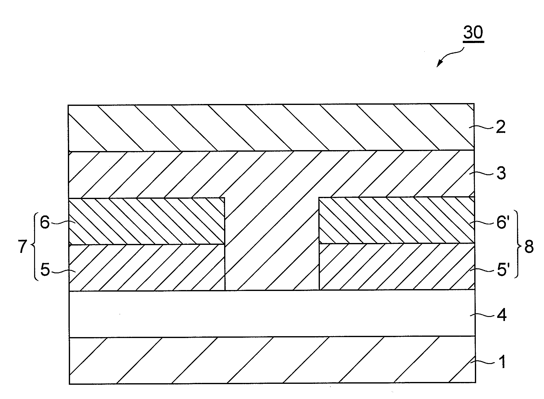
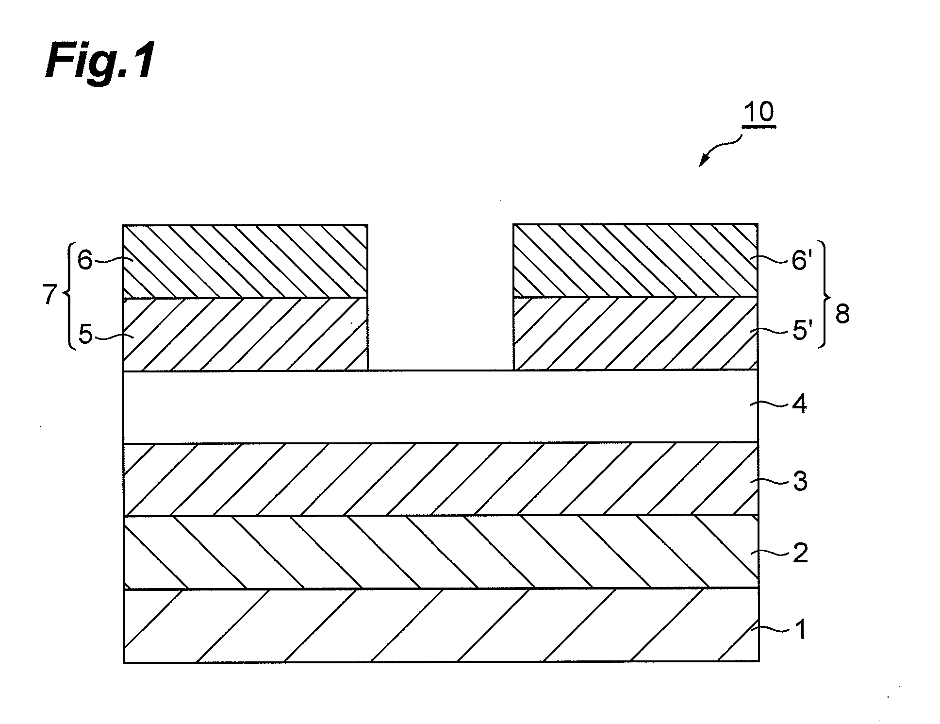
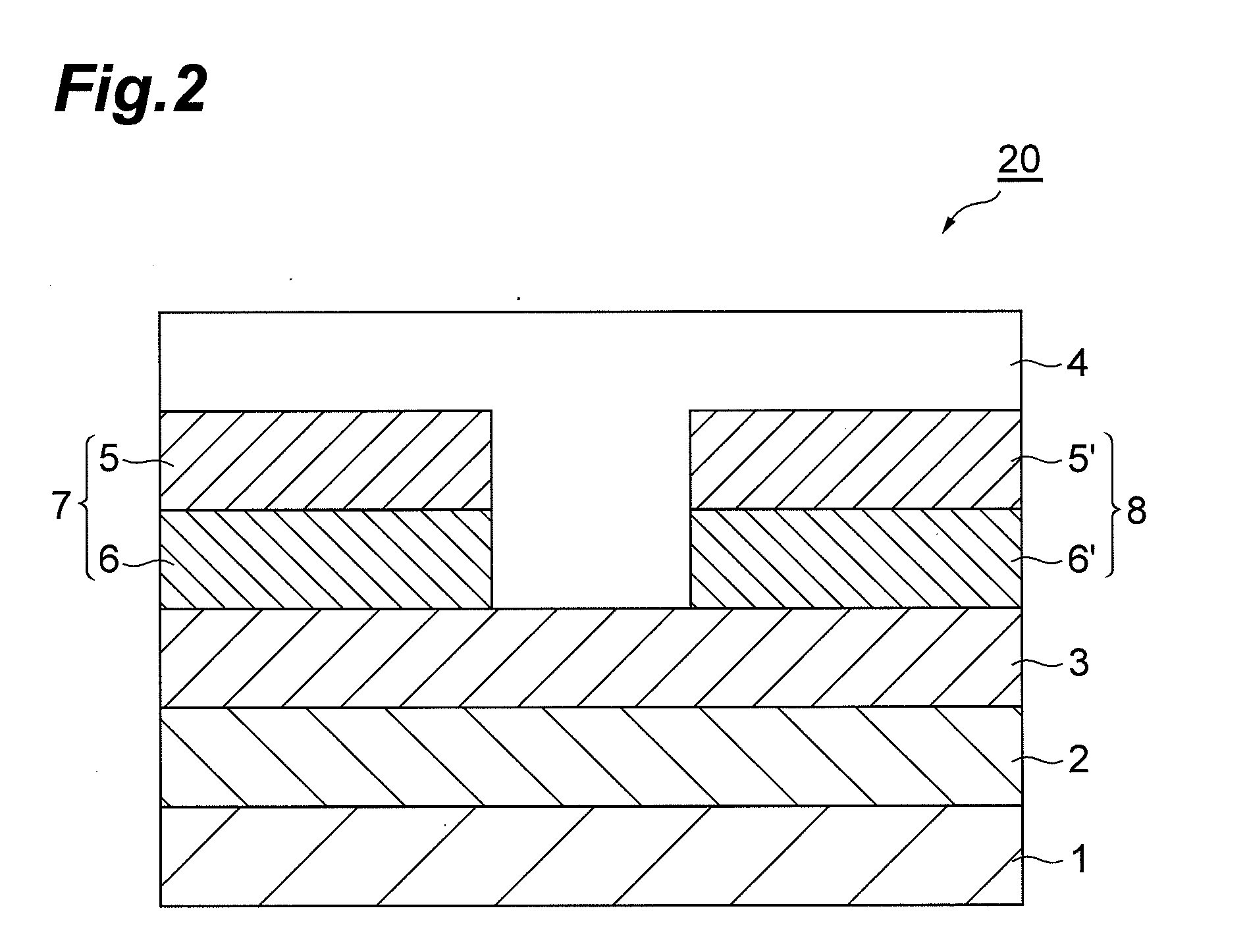
Image

Examples
synthesis example 1
[0061]2,7-dibromo-9,9-dioctylfluorene (26 g, 0.047 mol), 2,7-dibromo-9,9-diisopentylfluorene (5.6 g, 0.012 mol), and 2,2′-bipyridyl (22 g, 0.141 mol) were dissolved in 1600 mL of dehydrated tetrahydrofuran, and then, nitrogen bubbling was performed for nitrogen substitution in the system. Under a nitrogen atmosphere, bis(1,5-cyclooctadiene)nickel(0)[Ni(COD)2] (40 g, 0.15 mol) was added to this solution, the temperature of the solution was increased to 60° C., and the solution was reacted for 8 hours. After reaction, this reaction solution was cooled to room temperature (about 25° C.) and dropped into a mixed solution of 200 mL of 25 wt % aqueous ammonia / 1200 mL of methanol / 1200 mL of ion exchange water. The solution was stirred for 30 minutes, and then, the deposited precipitation was filtered and air-dried. Subsequently, the precipitation was dissolved in 1100 mL of toluene, and then, filtration was performed. The filtrate was dropped into 3300 mL of methanol, which was then stirre...
synthesis example 2
[0062]2,7-dibromo-9,9-di-n-octylfluorene and 5,5′-dibromo-2,2′-bithiophene were used, and these monomers were reacted in the presence of a palladium catalyst by a method described in U.S. Pat. No. 5,777,070 to synthesize a (2,7-9,9-di-n-octylfluorenediyl)(5,5′-dibromo-2,2′-bithiophene) alternating copolymer (polymer compound 2). The polymer compound 2 had a weight average molecular weight, in terms of polystyrene, of Mw=4×10⁴ and an ionization potential of 5.46 eV.
synthesis example 3
[0063]2,7-dibromo-9,9-di-n-octylfluorene and N,N-di(4-bromophenyl)-4-sec butylphenylamine were used, and these monomers were reacted in the presence of a palladium catalyst by the method described in U.S. Pat. No. 5,777,070 to synthesize a (2,7-9,9-di-n-octylfluorenediyl)(1,4-phenylene-((4-sec butylphenyl)imino)-1′,4′-phenylene) alternating copolymer (polymer compound 3). The polymer compound 3 had a weight average molecular weight, in terms of polystyrene, of Mw=4×10⁴ and an ionization potential of 5.43 eV.
PUM
| Property | Measurement | Unit |
|---|---|---|
| ionization potential | aaaaa | aaaaa |
| gate voltage | aaaaa | aaaaa |
| thickness | aaaaa | aaaaa |
Abstract
Description
Claims
Application Information
 - R&D
- Intellectual Property
- Life Sciences
- Materials
- Tech Scout
- Unparalleled Data Quality
- Higher Quality Content
- 60% Fewer Hallucinations
Browse by: Latest US Patents, China's latest patents, Technical Efficacy Thesaurus, Application Domain, Technology Topic, Popular Technical Reports.
© 2025 PatSnap. All rights reserved.Legal|Privacy policy|Modern Slavery Act Transparency Statement|Sitemap|About US| Contact US: help@patsnap.com