
Multi-Stacked Spin Transfer Torque Magnetic Random Access Memory and Method of Manufacturing the Same

a magnetic random access memory and multi-stacked technology, applied in the direction of digital storage, semiconductor devices, instruments, etc., can solve the problems of reducing affecting the performance of flash memory, and affecting the efficiency of flash memory, so as to improve the cell structure of stt-mram, minimize interference between adjacent mtjs, and secure the thermal stability of mtjs

Inactive Publication Date: 2010-01-28
SK HYNIX INC
View PDF1 Cites 35 Cited by
  • Summary
  • Abstract
  • Description
  • Claims
  • Application Information

AI Technical Summary

Benefits of technology

The present invention relates to improving a cell structure of a STT-MRAM device to secure thermal stability of a MTJ and minimize interference between adjacent MTJs, thereby improving its operating characteristics. The invention includes a multi-Stacked STT-MRAM device that includes a first MTJ connected to a first source / drain region of a first cell, a second MTJ connected to a second source / drain region of a second cell, and a common source line connected to both cells. The first and second MTJs may have different shapes, such as square, rectangular, or circular or oval. The method of manufacturing the multi-Stacked STT-MRAM device includes forming a first gate electrode and a second gate electrode over a semiconductor substrate, forming a common source line connected to a first source / drain region of a first cell, forming a first MTJ connected to a second source / drain region of a second cell, and forming a second MTJ connected to a third source / drain region of the second cell. The invention aims to improve the thermal stability of the MTJs and minimize interference between adjacent MTJs to enhance the performance of the STT-MRAM device.

Problems solved by technology

However, the flash memory has a slower speed than that of the DRAM and has a high operating voltage.
As a result, the cell size becomes larger, and the cell efficiency is degraded in comparison with other memories.
As a result, a disturbing phenomenon inverting neighboring cells occurs.
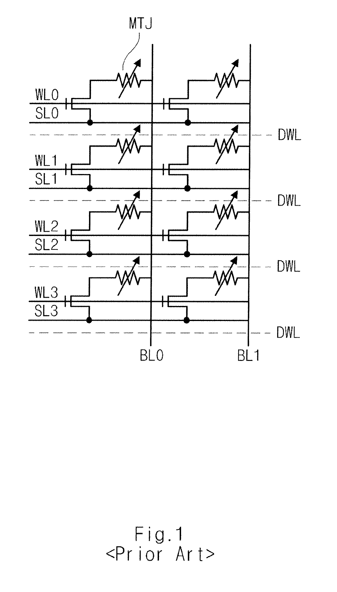
However, a magnetic field interference phenomenon occurs between the adjacent MTJs when the chip size becomes smaller.
As a result, there is a limit in reduction of the cell size of the conventional STT-MRAM.
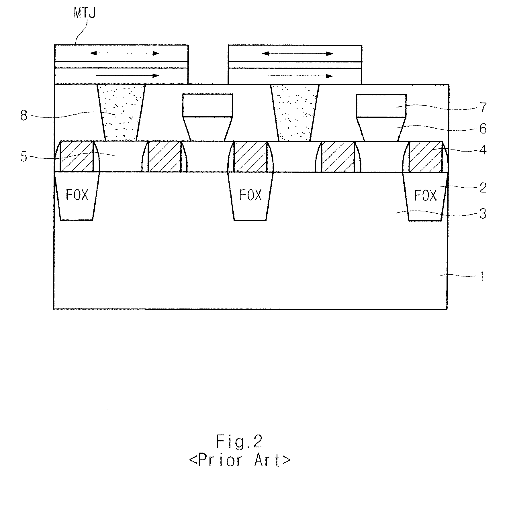
Also, there is a limit in increase of the size when the MTJs are formed over the same surface.

Method used


Image

  • Multi-Stacked Spin Transfer Torque Magnetic Random Access Memory and Method of Manufacturing the Same
  • Multi-Stacked Spin Transfer Torque Magnetic Random Access Memory and Method of Manufacturing the Same
  • Multi-Stacked Spin Transfer Torque Magnetic Random Access Memory and Method of Manufacturing the Same

Examples


Embodiment Construction

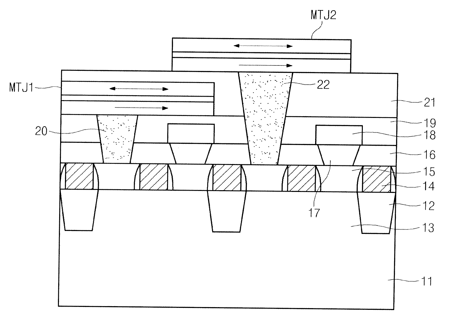
[0044]FIG. 3 is a cross-sectional diagram illustrating a STT-MRAM according to an embodiment of the present invention. A gate electrode 14 is formed over a silicon substrate 11 having a device isolation film 12 and an active region 13. A landing plug contact 15 is formed between the gate electrodes 14. A source line contact 17 is formed over the landing plug contact 15 positioned at one side of a source / drain region formed in both sides of the gate electrodes 14. Bottom electrode contacts 20 and 22 are formed over the landing plug contact 15 positioned at the other side of the source / drain region. A source line 18 is formed over the source line contact 17. A MTJ1 and MTJ2 are formed over the bottom electrode contacts 20 and 22, respectively. The source line 18 is formed to be straight in parallel with the gate electrode 14. Each of the MTJ1 and MTJ2 includes two magnetic layers and a tunnel barrier located between the two magnetic layers. The bottom magnetic layer includes a pinned ...


PUM


Abstract

A spin transfer torque magnetic random access memory (STT-MRAM) device comprises adjacent magnetic tunneling junctions (MTJ), respectively, formed in different layers, thereby preventing interference between the MTJs and securing thermal stability.

Description

CROSS-REFERENCES TO RELATED APPLICATIONS[0001]Priority is claimed to Korean patent application number 10-2008-0072823, filed on Jul. 25, 2008, which is incorporated by reference in its entirety.BACKGROUND OF THE INVENTION[0002]The present invention generally relates to a spin transfer torque magnetic random access memory (STT-MRAM) device, and more specifically, to a multi-stacked STT-MRAM device that includes magnetic tunneling junctions (MTJ) of adjacent cells, respectively, formed in different layers, and a method of manufacturing the same.[0003]Dynamic random access memory (DRAM) occupies the largest memory market. DRAM comprises a MOS transistor and a capacitor, which are paired, functioning as 1 bit. DRAM is a volatile memory that requires a periodic refresh operation in order not to lose data because the DRAM writes data by storing charges in the capacitor.[0004]As an example of non-volatile memory, a NAND / NOR flash memory does not lose a stored signal even when a power sourc...

Claims


Application Information

Patent Timeline
Patent Type & Authority Applications(United States)
IPC IPC(8): H01L21/8246H01L27/22H10B20/00H10B69/00
CPCH01L43/08H01L27/228G11C11/1659H10B61/22H10N50/10G11C11/15H10N50/01
Inventor HWANG, SANG MIN
Owner SK HYNIX INC
Learn More