
Microwave plasma processing apparatus

a plasma processing and microwave technology, applied in the direction of chemical vapor deposition coating, coating, electric discharge tube, etc., can solve the problems of large throughput, difficult to perform a plasma process uniformly over an entire substrate to be processed at a high processing speed, non-uniform plasma formation, etc., to achieve high elasticity, fixed and supported more effectively, and sufficient electrical contact area

Inactive Publication Date: 2009-12-10
TOKYO ELECTRON LTD
View PDF7 Cites 10 Cited by
  • Summary
  • Abstract
  • Description
  • Claims
  • Application Information

AI Technical Summary

Benefits of technology

[0022]The present invention is purposed to generate uniform plasma by preventing changes in locations of slot plate of a microwave antenna constituting a microwave plasma processing apparatus and preventing variations in desired propagation of microwave.

Problems solved by technology

However, these conventional plasma processing apparatuses have problems such as non-uniform plasma formation and difficulty of performing a plasma process uniformly over an entire substrate to be processed at a high processing speed, that is, large throughput due to limited regions with high electron densities.
The problems become more significant especially when a substrate having a large diameter is processed.
Furthermore, such conventional plasma processing apparatuses have essential problems such as damages inflicted to semiconductor devices formed on a substrate to be processed due to high electron temperature, severe metal contamination due to sputtering on sidewalls of a processing chamber, etc.
Therefore, it becomes more and more difficult for a conventional plasma processing apparatus to fulfill strict demands for finer semiconductor devices, finer liquid crystal displays, and improved productivity of the same.
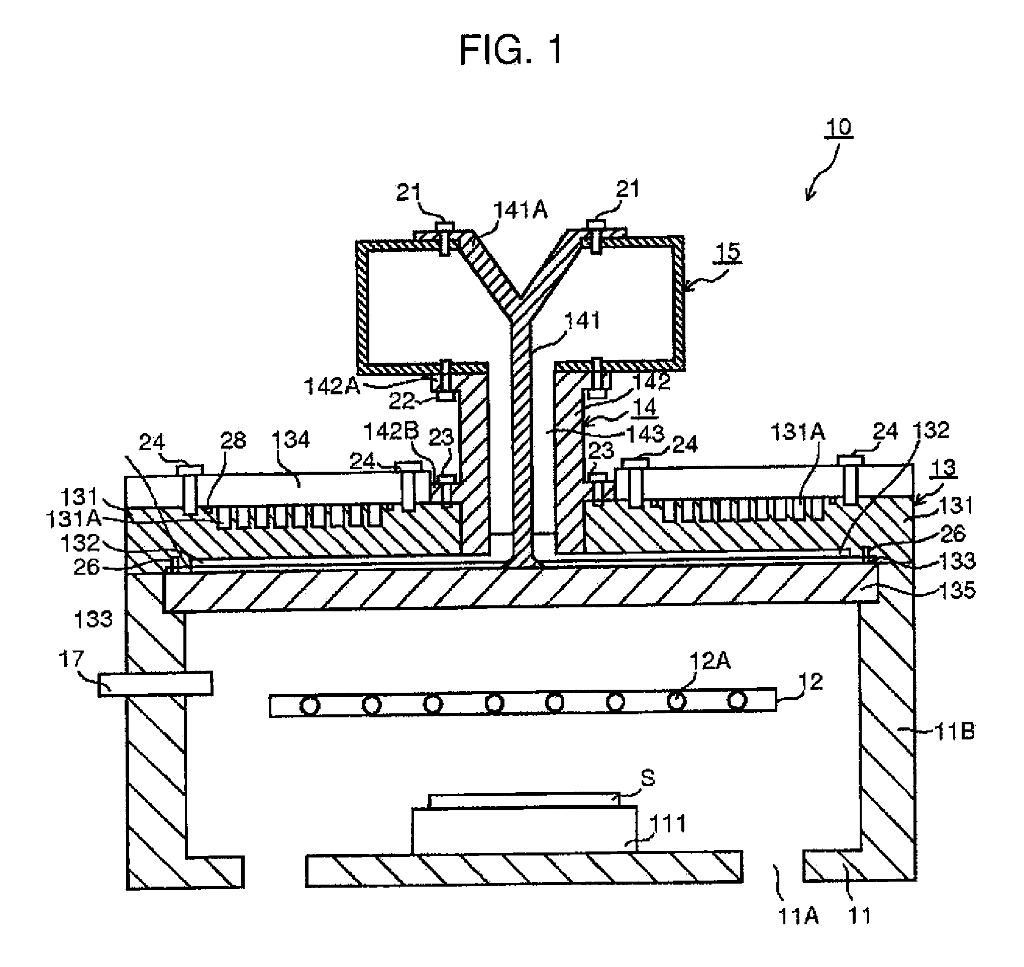
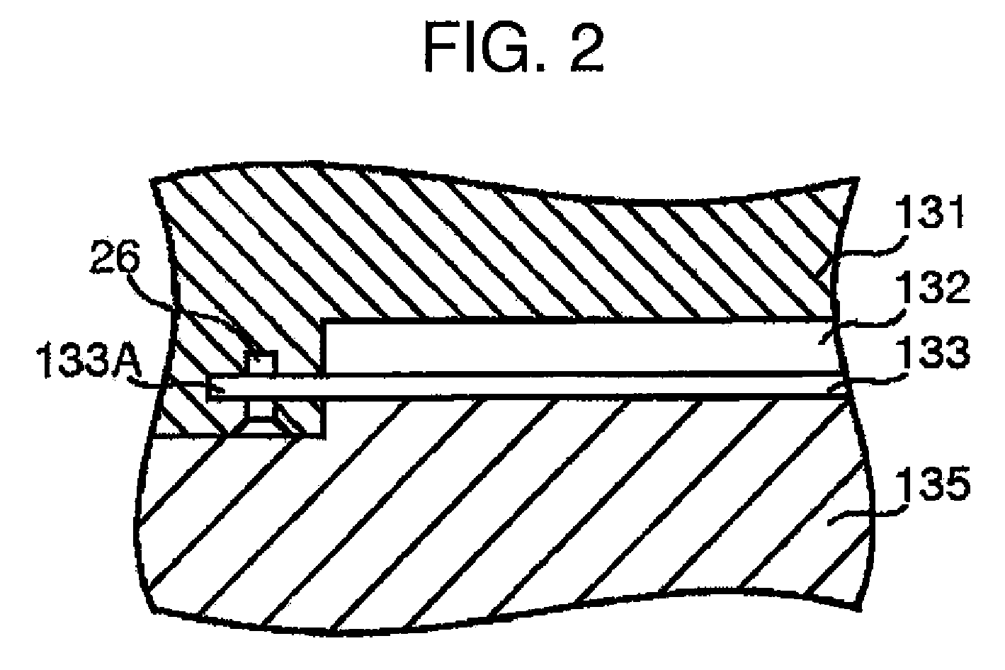
Therefore, if a position of a slot changes as described above, the emission state of microwave from the slot changes, then the microwaves cannot be uniformly emitted into the processing container 11, and thus the process on the substrate S cannot be uniformly performed.
As a result, the stability or reliability of a microwave plasma processing apparatus is deteriorated.

Method used


Image

  • Microwave plasma processing apparatus
  • Microwave plasma processing apparatus
  • Microwave plasma processing apparatus

Examples


Embodiment Construction

[0042]The attached drawings for illustrating exemplary embodiments of the present invention are referred to in order to gain a sufficient understanding of the present invention, the merits thereof, and the objectives accomplished by the implementation of the present invention. Hereinafter, the present invention will be described in detail by explaining exemplary embodiments of the invention with reference to the attached drawings.

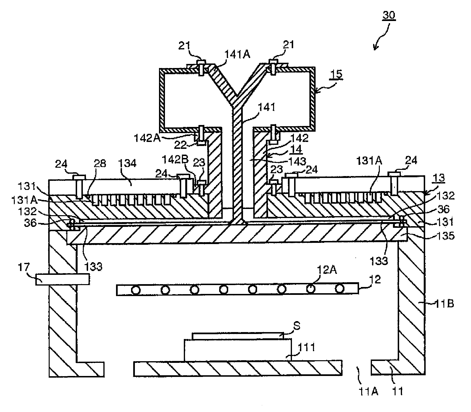
[0043]FIG. 3 is a sectional view of an example of the configuration of a microwave plasma processing apparatus 30 according to an embodiment of the present invention, and FIG. 4 is a detailed sectional view showing that an end 133A of a slot plate 133 and a top plate 135 of an microwave antenna 13 of the microwave plasma processing apparatus 30 shown in FIG. 3 are fixed. Furthermore, the shape of a microwave plasma processing apparatus, particularly, a microwave antenna thereof is circular when viewed from above. Although not shown, the shape of each of the...


PUM

PropertyMeasurementUnit
gate lengthsaaaaaaaaaa
temperatureaaaaaaaaaa
elasticityaaaaaaaaaa

Abstract

An end of the slot plate of the microwave antenna, which constitutes a microwave plasma processing apparatus, is held and fixed by being held between a pair of metal bodies.

Description

CROSS-REFERENCE TO RELATED PATENT APPLICATIONS[0001]This application claims the benefit of Japanese Patent Application No. 2008-149401, filed on Jun. 6, 2008, in the Japan Patent Office, the disclosure of which is incorporated herein in its entirety by reference.BACKGROUND OF THE INVENTION[0002]1. Field of the Invention[0003]The present invention relates to a microwave plasma processing apparatus that can be highly appropriate for the fabrication of ultra-fine semiconductor devices or the fabrication of high-resolution flat panel display apparatuses that have liquid crystal display devices.[0004]2. Description of the Related Art[0005]A plasma processing process and a plasma processing apparatus are essential technologies for the fabrication of an ultra-fine semiconductor device, which has gate lengths close to or smaller than 0.1 μm and is often referred as a deep submicron device or a deep sub-quarter micron device, or the fabrication of a high-resolution flat panel display apparat...

Claims


Application Information

Patent Timeline
Patent Type & Authority Applications(United States)
IPC IPC(8): H01L21/465C23C16/511
CPCH01J37/3222H01J37/32192H01J37/3244
Inventor NISHIMOTO, SHINYASAKATA, KAZUNARI
Owner TOKYO ELECTRON LTD
Learn More