
Method for constructing a phase conjugate mirror

a phase conjugate mirror and mirror technology, applied in the direction of crystal growth process, instruments, transportation and packaging, etc., can solve the problems of difficult frequency-scanning, and difficult to achieve monolithic integration. achieve the effect of neutralizing anomalous internal reflections

Inactive Publication Date: 2009-11-05
HENRICHS JOSEPH REID
View PDF1 Cites 9 Cited by
  • Summary
  • Abstract
  • Description
  • Claims
  • Application Information

AI Technical Summary

Benefits of technology

[0029]Various aspects of the invention are novel, non-obvious, and provide various advantages. While the actual nature of the invention covered herein, may only be determined with reference to the claims appended hereto, certain features, which are characteristic of the preferred embodiment disclosed herein, are described briefly as follows:
[0030]a) One feature of the present invention is a corner-cube array that includes a (111) semiconductor substrate and a number of semiconductor crystalline projections generally extending perpendicular from the substrate wafer surface on axis along the (111) crystal lattice direction. The projections each have a corner-cube shape with three generally planar surfaces. The surfaces are generally mutually perpendicular and generally correspond to (100), (010), and (001) crystal axis faces;
[0031]b) Another feature of the invention provides for a semiconductor substrate that has a cubic crystalline lattice structure, and a number of non-crystalline (i.e., polycrystalline or sometimes called amorphous semiconductor material), which are generally formed apart from one another in a predetermined pattern along the growth plane of said substrate. These non-crystalline areas are formed when the semiconductor material used to comprise the substrate is made none crystalline as the result of ion and/or proton implantation, which is projected through a mask to produce a predefined pattern of polycrystalline material along the growth plane of the substrate. These amorphous polycrystalline implantation sites made to form within the substrate will be used to spatially control further semiconductor crystal growth on the substrate wafer. Wherein, a number of semiconductor crystalline corner-cube projections will be made to grow out from the growth pla

Problems solved by technology

This makes the use of active OPC in laser systems problematic and costly, with monolithic integration being nearly impossible in semiconductor laser diodes.
Additionally, current forms of active OPC (e.g., Four-Wave Mixing, Three-Wave Mixing, Raman Scattering, and Stimulated Brillouin Scattering) suffer from what is sometimes called the frequency-scanning problem, which is typically solved using complex and costly laser-cavity configurations and complex design schemes.
However, in order for a corner-cube array to provide OPC in a device such as a semiconductor laser-diode it must first meet several strict criteria; e.g., such as structural coherency, unobstructed external / internal retro-reflection / refraction, all of which is very hard to achieve for sub-millimeter sized structures.
Consequently, if used to provide total internal reflection, these pads (due to the high contrast in refraction exhibited between Silicon-Dioxide or Silicon-Nitride and Silicon) cause anomalous reflections to occur in front of the corner-cube array; thus, neutralizing the OPC capability of the passive PCM (i.e., anomalous reflections cause spatial hole burning to occur for the cavity, which seriously degrades the performance of the laser).
Alternatively, if a corner-cube array, as provided by Neudeck, et al., were used to provide external reflection in the cavity of a laser-diode, the laser-diode would fail to laze due to optical losses that occur at the air / metal interface of the light reflecting surface of the corner-cube array.
Each of these techniques has various limitations, especially when both small corner-cube dimensions and high optical performance are desired.
However, it is not presently possible to produce cube-corner geometries that have very-high coherency and effective apertures at low-entrance angles using direct machining construction techniques.

Method used


Image

  • Method for constructing a phase conjugate mirror
  • Method for constructing a phase conjugate mirror
  • Method for constructing a phase conjugate mirror

Examples


Embodiment Construction

—FIGS. 1, 2, 3, 4, AND 5—PREFERRED EMBODIMENT

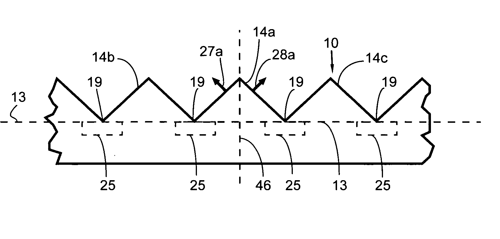
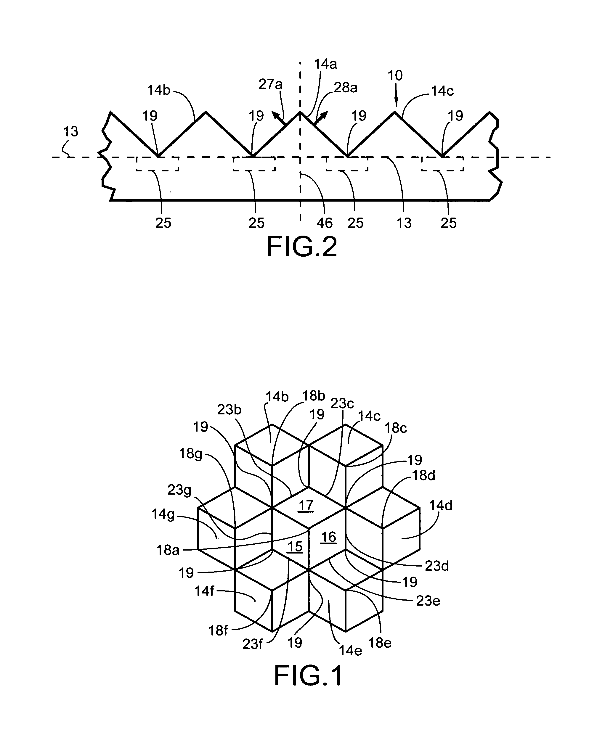
[0051]For the purposes of promoting an understanding of the principles of the invention, reference will now be made to the embodiment illustrated in the drawings and specific language will be used to describe the same. It will nevertheless be understood that no limitation of the scope of the invention is thereby intended. Any alterations and further modifications in the described device, and any further applications of the principles of the invention as described herein are contemplated as would normally occur to one skilled in the art to which the invention relates. FIG. 1 depicts a crystalline corner-cube array device 10 of the present invention. Device 10 has a substrate 11 supporting a corner-cube array 10.

[0052]Further, FIG. 1 provides a cutaway view of substrate 11 corresponding to the removal of a part of corner-cube array 10. Substrate 11 is formed from a semiconductor material (e.g., GaAs, InP), having a common cubic crystalline ...


PUM

PropertyMeasurementUnit
Lengthaaaaaaaaaa
Pressureaaaaaaaaaa
Angleaaaaaaaaaa

Abstract

A method that provides for a phase conjugate mirror 10 having a gallium-arsenide substrate 11 with a generally cubic crystalline lattice and a number of gallium-arsenide crystal projections 14 extending from said substrate 11, the projections each having three generally planar surfaces 15, 16, 17, where the surfaces each being generally obliquely oriented with respect to a plane of said substrate 11, the plane substantially corresponding to a (111) crystal face, the projections 14 being oriented along the plane 13 to provide a predetermined corner-cube array pattern 10, the device including a number of implant sites 25 spaced apart from one another along the substrate 11 to define a pattern 40, and forming a number of corner-cubes articles having a shape substantially corresponding to the corner-cube array 10 pattern 40, wherein the articles each have a number of cube-corner projections 14 spaced apart from each other by a minimum distance of 1 micron. Further, providing for a method of slowing annealing that re-crystallizes the implant sites 25, which located between and slightly underneath the corner-cube projections, where the implant sites 25 are embedded within the substrate material.

Description

BACKGROUND OF THE INVENTION[0001]1. Field of the Invention[0002]“Optical Phase Conjugation” (OPC) is described by optical and laser physicists as being a nonlinear optical effect that can be used to precisely reverse both the direction of propagation and the overall phase for each plane-wave in an arbitrary beam of light.[0003]2. Background of the Invention[0004]A beam of light, being retro-reflected by a “Phase Conjugation Mirror” (PCM), retraces its path of propagation backwards to its point of origin. OPC is an optical process that is expressed by the equationkin=kout.[0005]When used to provide retro-reflection in an optical feedback system, such as the system used in lasers, a PCM provides for some highly desirable effects; e.g., suppression of “Amplified Spontaneous Emission” (ASE), the neutralization of filamentation (i.e., so called self-focusing effect problem by those well versed in the art) that occurs in broad-area high-powered laser-diodes (e.g., Broad-Area configured Ve...

Claims


Application Information

Patent Timeline
IPC IPC(8): G02B5/124C30B23/04C25D7/08B32B7/00
CPCC25D1/10C30B23/02C30B29/42Y10T117/10G02B5/124Y10T428/24174G02B1/02
Inventor HENRICHS, JOSEPH REID
Owner HENRICHS JOSEPH REID
Learn More