
Method and system for overlay correction during photolithography

a photolithography and overlay technology, applied in the field of manufacturing objects, can solve the problems of limiting the chemicals to which the structure can be exposed, affecting the quality of the image, so as to reduce the level of particles and potential defects, increase the wafer yield, and reduce the level of particle and potential defects

Active Publication Date: 2009-09-17
MIRADIA INC
View PDF35 Cites 1 Cited by
  • Summary
  • Abstract
  • Description
  • Claims
  • Application Information

AI Technical Summary

Benefits of technology

[0008]Many benefits are achieved by way of the present invention over conventional techniques. For example, the present technique reduces the number of process steps and the corresponding process cycle time for lithography processes (as much as 50%) and reduces the level of particles and potential defects associated with conventional photoresist rework processes, which in turn helps to increase production throughput. Additionally, embodiments of the present invention are applicable to general lithography steps in both CMOS and / or MEMS device fabrication flows in which a stringent overlay specification is utilized, but no established pre-correction values are available. Moreover, embodiments increase wafer yield and increase overlay error correction accuracy in comparison with conventional rework processes. For example, some embodiments of the present invention eliminate photoresist rework processes through the use of the described overlay error correction techniques. Furthermore, embodiments of the present invention help to eliminate potential damage to portions of semiconductor devices (e.g., mirror stacks) that are processed using a conventional photoresist rework process. Depending upon the embodiment, one or more of these benefits may be achieved. These and other benefits will be described in more detail throughout the present specification and more particularly below.

Problems solved by technology

The photoresist rework described above presents problems for semiconductor processes including the use of sacrificial materials.
For example, the presence of the sacrificial materials at various positions in the structure may limit subsequent temperature processes to particular temperatures and may limit the chemicals to which the structure can be exposed, even when the sacrificial material (e.g., photoresist) is fully encapsulated.
Thus, when downstream processes involve overlay correction, which as discussed above, is common when device alignment is an important parameter, stripping of the photoresist can become a challenging and time consuming task.
Additionally, the conventional process can introduce particles, which adversely impact device yield by increasing the defect density.

Method used


Image

  • Method and system for overlay correction during photolithography
  • Method and system for overlay correction during photolithography
  • Method and system for overlay correction during photolithography

Examples


Embodiment Construction

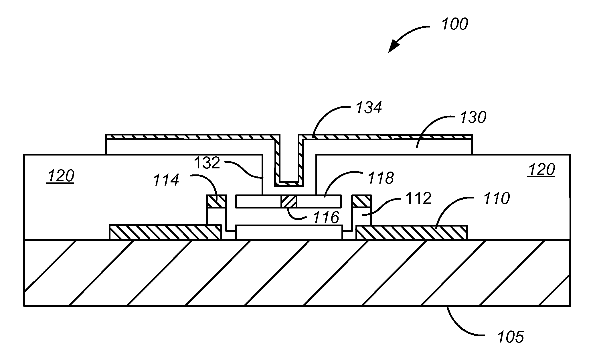
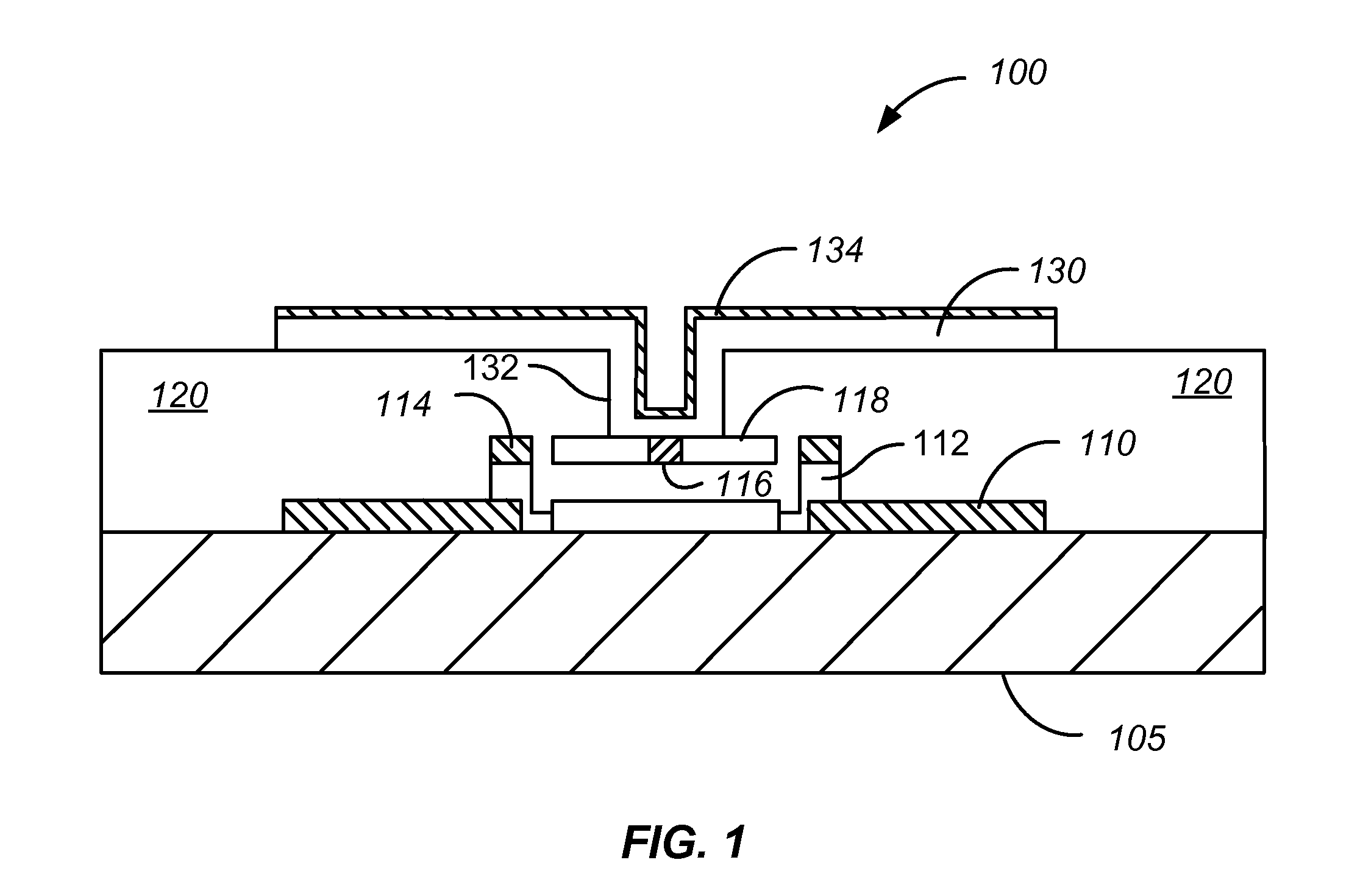
[0016]FIG. 1 is a simplified schematic diagram illustrating a semiconductor device at an intermediate stage of processing. As illustrated in FIG. 1, a micro-mirror 100 for display applications is illustrated at one portion of a process flow during the spatial light modulator (SLM) fabrication process. A CMOS wafer 105 is illustrated after a via formation process. Bottom electrode layer 110, which is formed using a low temperature PVD metal deposition process, is provided on the CMOS wafer 105. The bottom electrode layer is fabricated in an embodiment using deposition, photolithography, and etching processes. As an example, the bottom electrode layer 110 may include a multi-layer metal stack such as 1,000 Å of titanium nitride (TiN), 8,000 Å of aluminum, and another 1,000 Å of TiN.

[0017]Sacrificial photoresist material 120 is formed over the CMOS substrate and the bottom electrode layer. The sacrificial photoresist material 105 encapsulates an HDP insulator layer, 112 coupled to the ...


PUM

PropertyMeasurementUnit
roughnessaaaaaaaaaa
temperatureaaaaaaaaaa

Abstract

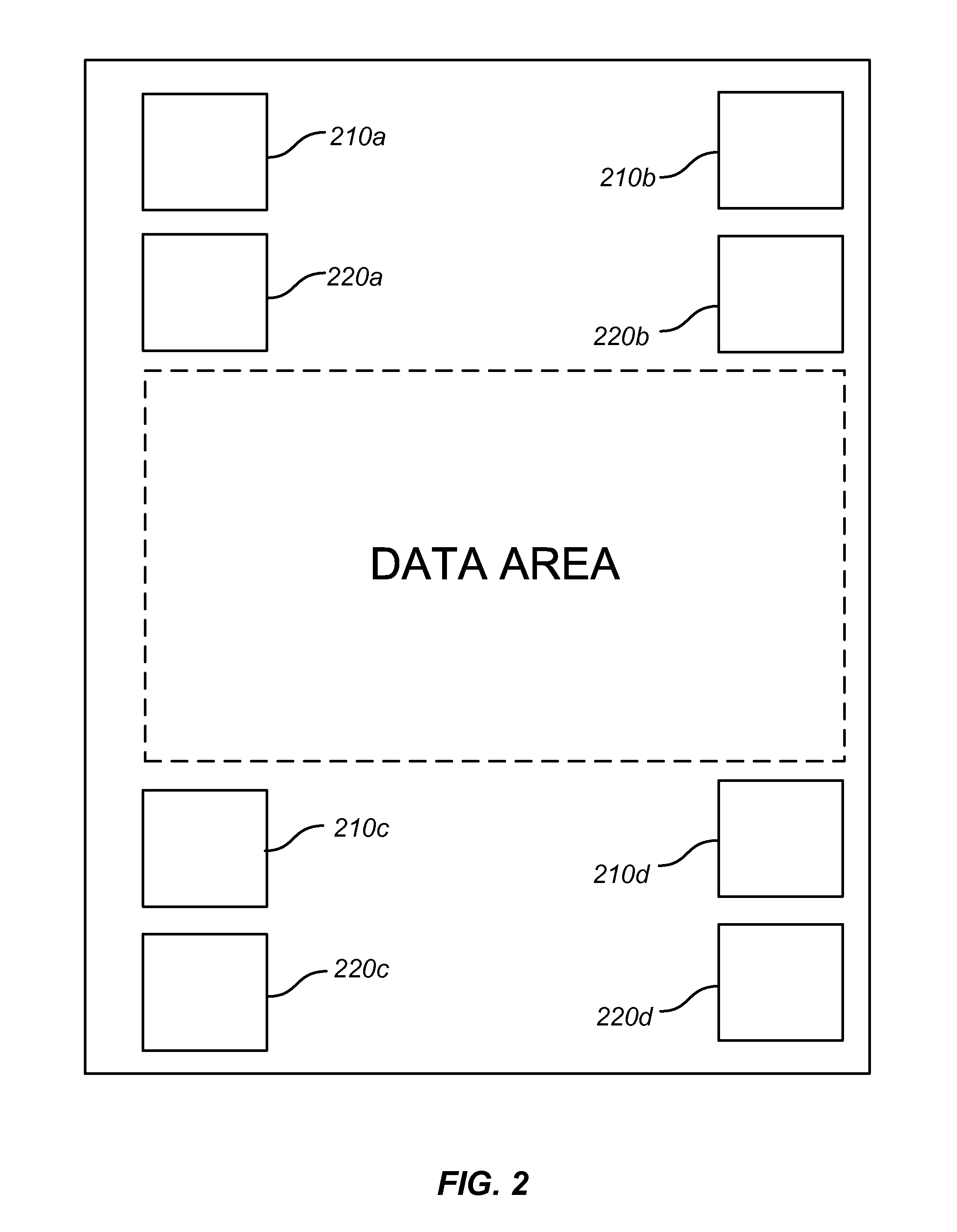
A method of performing overlay error correction includes forming a photoresist layer over a substrate and exposing a first set of apertures to incident radiation. The method also includes determining an overlay error associated with the first set of apertures and determining an overlay correction as a function of the determined overlay error. The method further includes exposing a data area and a second set of apertures. The data area and the second set of apertures are exposed based, in part, on the determined overlay correction. Moreover, the method includes verifying the determined overlay correction.

Description

BACKGROUND OF THE INVENTION[0001]This present invention relates generally to manufacturing objects. More particularly, the invention relates to a method and system for measuring and correcting overlay error during photolithographic processing. Merely by way of example, the invention has been applied to the formation and exposure of multiple overlay measurement features. The method and system can be applied to photolithographic processing of CMOS structures as well as other devices, for example, micro-electromechanical systems (MEMS) including sensors, detectors, and displays.[0002]During various semiconductor manufacturing processes, there is a need to control the alignment between various layers present in the semiconductor devices. For example, in the semiconductor manufacturing industry, it is common to fabricate electronic devices by forming and patterning a series of layers (e.g., semiconductors, insulators, metals, and the like) using photolithography processes. As a particula...

Claims


Application Information

Patent Timeline
Patent Type & Authority Applications(United States)
IPC IPC(8): G03F7/26
CPCG03F7/70633
Inventor YANG, XIAOWANG, YUXIANGWANG, YEPAYNE, JUSTINJI, WOOK
Owner MIRADIA INC
Learn More