
Void-free copper filling of recessed features using a smooth non-agglomerated copper seed layer

Active Publication Date: 2009-09-10
TOKYO ELECTRON LTD
View PDF60 Cites 52 Cited by
  • Summary
  • Abstract
  • Description
  • Claims
  • Application Information

AI Technical Summary

Benefits of technology

[0008]A method is provided for controlling copper agglomeration on a substrate and for forming void-free bulk copper metal filling of recessed features in integrated circuits. The method utilizes a metal-containing wetting film that enables formation of a smooth copper metal seed layer and void-free copper metal filling of small recessed features with high-aspect-ratios.
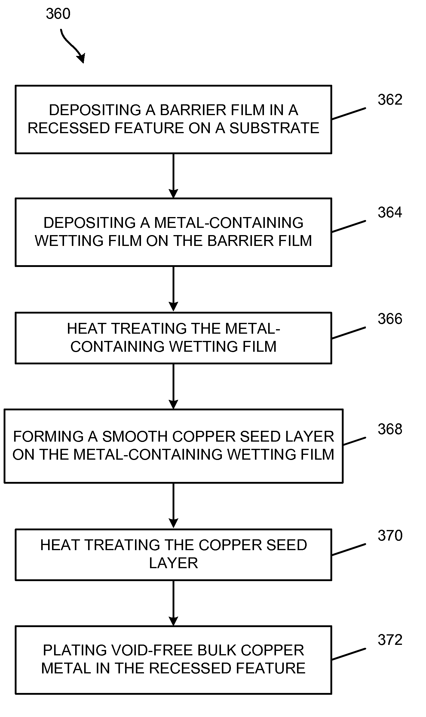
[0010]According to one embodiment of the invention, a method is provided for processing a substrate. The method includes providing a substrate having a topography including a top surface and at least one recessed feature containing at least a sidewall surface and a bottom surface; depositing a barrier film on the substrate topography; and depositing a metal-containing wetting film on the barrier film. The method further includes physical vapor depositing copper metal on the metal-containing wetting film, where the metal-containing wetting film prevents agglomeration of the copper metal and where the substrate temperature is greater than 0° C. and causes the copper metal to form a smooth copper metal seed layer on the metal-containing wetting film; and plating void-free bulk copper metal in the at least one recessed feature.

Problems solved by technology

As the width of metal lines are scaled down to smaller submicron and even nanometer dimensions, the small features are difficult to fill with bulk metal, leading to formation of voids in the bulk metal filling and electromigration (EM) failure, which may lead to open and extruded metal lines.
However, copper metal cannot be put in direct contact with dielectric materials since copper metal has poor adhesion to the dielectric materials and copper metal is known to easily diffuse into common integrated circuit materials such as silicon and dielectric materials where copper is a mid-bandgap impurity.
Furthermore, oxygen can diffuse from an oxygen-containing dielectric material into copper metal, thereby decreasing the electrical conductivity of the copper metal.
However, a tantalum adhesion layer is easily oxidized which reduces its copper wetting properties.
The copper metal agglomeration is detrimental to the subsequent copper metal plating process and frequently results in formation of voids in the plated bulk copper metal.
However, the low substrate temperatures result in rough or irregular copper metal layers and do not eliminate the copper metal agglomeration on the tantalum adhesion layer and the formation of voids in the plated bulk copper metal.

Method used


Image

  • Void-free copper filling of recessed features using a smooth non-agglomerated copper seed layer
  • Void-free copper filling of recessed features using a smooth non-agglomerated copper seed layer
  • Void-free copper filling of recessed features using a smooth non-agglomerated copper seed layer

Examples


Embodiment Construction

[0018]A method is provided for controlling copper agglomeration on a substrate and for providing void-free bulk copper metal filling of recessed features in integrated circuits. In one embodiment, deposition of a smooth copper metal seed layer by physical vapor deposition in a recessed feature is facilitated by an underlying metal-containing wetting film. The metal-containing wetting film can contain a metal film that provides a small contact angle with an overlaying copper metal film, thereby providing good wetting of copper metal on the metal-containing wetting film. The metal-containing wetting film can, for example, contain amorphous, polycrystalline, or crystalline ruthenium metal (Ru), palladium metal (Pd), rhodium metal (Rh), or silver metal (Ag), or a combination thereof. In other examples, the metal-containing wetting film can contain compounds of these metals and nitrogen, oxygen, carbon, boron, or phosphorus, for example. The processing methods presented in embodiments of...


PUM

PropertyMeasurementUnit
Temperatureaaaaaaaaaa

Abstract

A method is provided for controlling copper agglomeration on a substrate and for forming void-free bulk copper metal filling of recessed features in integrated circuits. In one embodiment, the method includes providing a substrate having a topography including a top surface and at least one recessed feature comprising at least a sidewall surface and a bottom surface, depositing a barrier film on the substrate topography, and depositing a metal-containing wetting film on the barrier film. The method further includes physical vapor depositing copper metal on the metal-containing wetting film, where the substrate temperature is sufficiently high to form a smooth copper metal seed layer on the metal-containing wetting film. Void-free bulk copper metal may be plated in the at least one recessed feature.

Description

CROSS-REFERENCE TO RELATED APPLICATIONS[0001]The present invention is related to U.S. patent application Ser. No. 11 / 693,298, (Attorney docket no. TTCA-178), filed Mar. 29, 2007 and entitled METHOD OF FORMING LOW-RESISTIVITY COPPER FILM STRUCTURES. The present invention is related to U.S. patent application Ser. No. 11 / 864,566, (Attorney docket no. TTCA-229), filed Sep. 28, 2007 and entitled VOID-FREE COPPER FILLING OF RECESSED FEATURES FOR SEMICONDUCTOR DEVICES. The entire content of these applications is incorporated herein by reference.FIELD OF THE INVENTION[0002]The invention relates to manufacturing of semiconductor devices, and more particularly to controlling copper agglomeration on a substrate and processing methods for void-free bulk copper metal (Cu) filling of recessed features in integrated circuits.BACKGROUND OF THE INVENTION[0003]An integrated circuit (IC) contains various semiconductor devices and a plurality of conducting metal paths that provide electrical power to ...

Claims


Application Information

Patent Timeline
IPC IPC(8): C23C16/00
CPCH01L21/2855H01L21/76843H01L21/76864H01L21/76873H01L23/53238H01L2924/0002H01L2221/1089H01L2924/00
Inventor SUZUKI, KENJIGOMI, ATSUSHIJOMEN, MIHO
Owner TOKYO ELECTRON LTD
Learn More