
Method of growing semi-polar nitride single crystal thin film and method of manufacturing nitride semiconductor light emitting diode using the same

a technology of semi-polar nitride and single crystal thin film, which is applied in the direction of polycrystalline material growth, crystal growth process, chemically reactive gas growth, etc., can solve the problems of lowering the luminous efficiency of the light emitting diode, difficult to grow the nitride single crystal thin film into a semi-polar plane, and difficult to realize the light emitting diode using a long wavelength element. , to achieve the effect of improving the luminous efficiency of the ligh

Active Publication Date: 2009-06-18
SAMSUNG ELECTRONICS CO LTD
View PDF2 Cites 19 Cited by
  • Summary
  • Abstract
  • Description
  • Claims
  • Application Information

AI Technical Summary

Benefits of technology

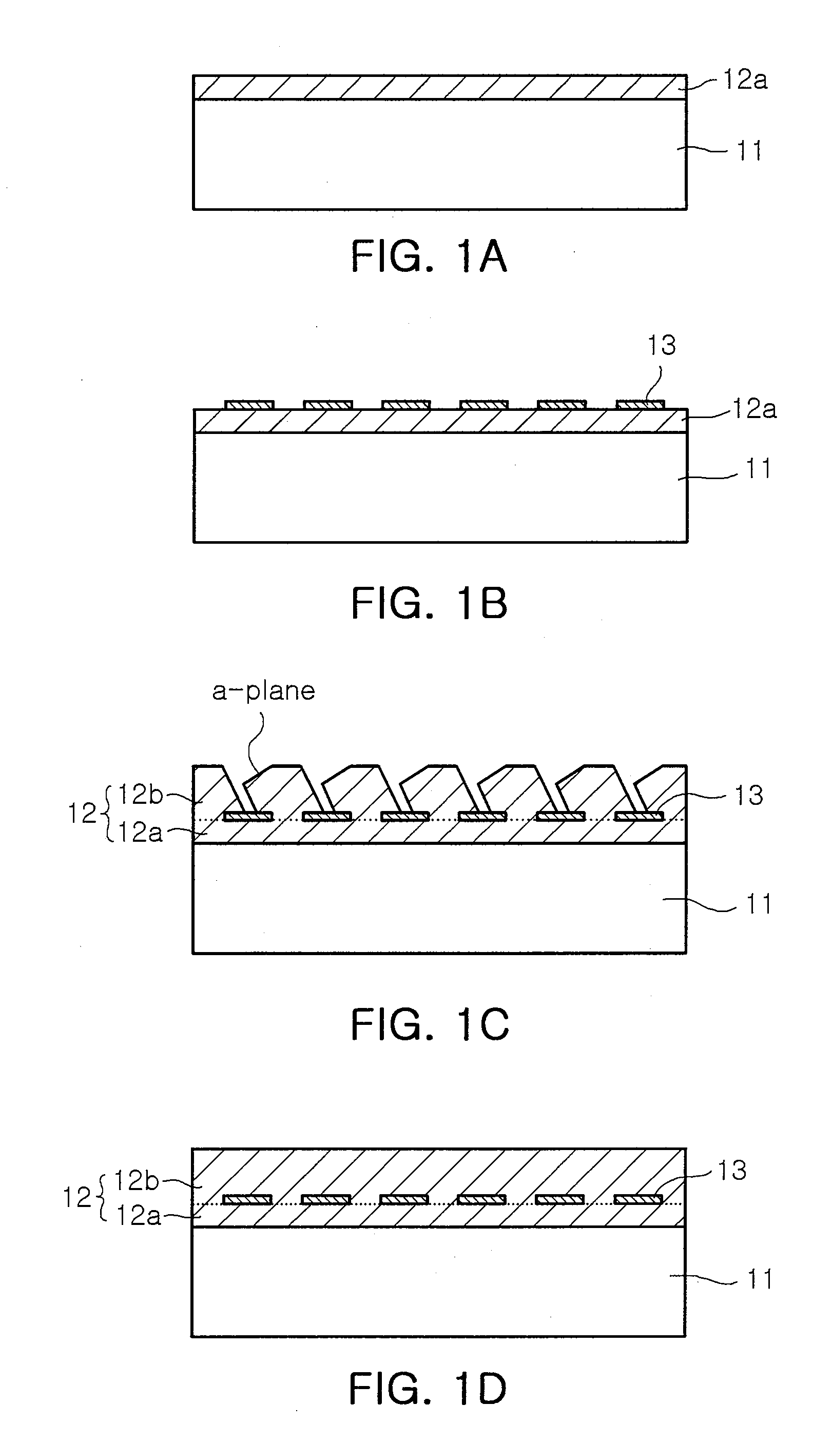
[0009]An aspect of the present invention is to provide a method of growing a semi-polar nitride single crystal thin film, in which the semi-polar nitride single crystal thin film is grown twice on an m-plane hexagonal system single crystal substrate at different lateral growth rates in a lateral direction, thereby having a (11 22) plane and high crystallinity.
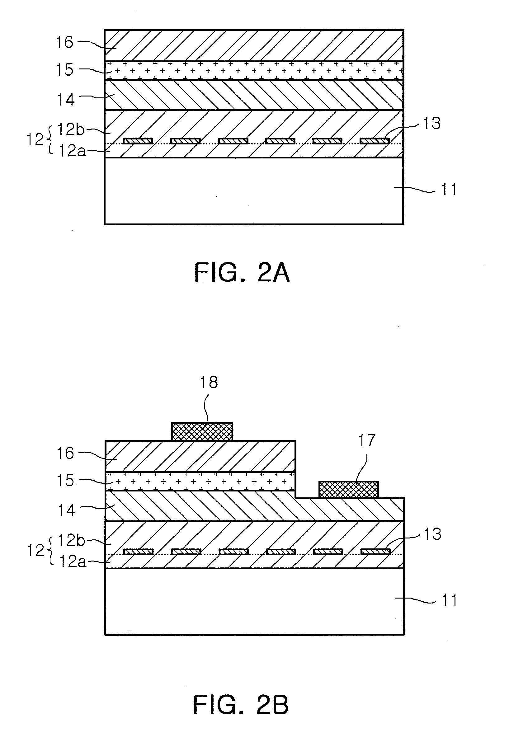
[0010]Another aspect of the present invention is to provide a method of manufacturing a nitride semiconductor light emitting diode, in which a light emitting structure is formed on a semi-polar nitride single crystal thin film, thereby improving luminous efficiency.
[0032]According to the present invention, the semi-polar nitride single crystal thin film is grown twice on the m-plane hexagonal system single crystal substrate at different lateral growth rates in a lateral direction, thereby having the (11 22) plane and the high crystallinity.
[0033]Further, when the light emitting diode is manufactured, the light emitting structure is formed on this nitride single crystal thin film, so that the nitride single crystal thin film prevents an internal electric field from being generated, and increases a recombination rate of electrons and holes which are required to emit light. Thus, the luminous efficiency of the light emitting diode can be improved, and the light can be emitted with a longer wavelength, so that the reliability of the light emitting diode can be improved.

Problems solved by technology

In this case, the internal electric field inside the light emitting diode is responsible for reduction in the recombination rate of electrons and holes, thereby lowering luminous efficiency of the light emitting diode.
Thus, it is difficult to realize the light emitting diode using a long wavelength element.
However, when the c-plane hexagonal system single crystal substrate is used, it is difficult to grow the nitride single crystal thin film into a semi-polar plane.
Further, when the semi-polar nitride single crystal thin film is grown, crystal defects occur due to a lattice constant difference between the substrate and the semi-polar nitride single crystal thin film.
These crystal defects induce non-radiative recombination in the event of the operation of the light emitting diode, thereby generating much heat.

Method used


Image

  • Method of growing semi-polar nitride single crystal thin film and method of manufacturing nitride semiconductor light emitting diode using the same
  • Method of growing semi-polar nitride single crystal thin film and method of manufacturing nitride semiconductor light emitting diode using the same
  • Method of growing semi-polar nitride single crystal thin film and method of manufacturing nitride semiconductor light emitting diode using the same

Examples


Embodiment Construction

[0040]Exemplary embodiments of the present invention will now be described in greater detail with reference to the accompanying drawings.

[0041]FIGS. 1A through 1D are process diagrams for explaining a method of growing a nitride single crystal thin film according to an embodiment of the present invention. Referring to FIG. 1A, a semi-polar nitride single crystal base layer 12a is deposited on an m-plane hexagonal system single crystal substrate 11. Here, the hexagonal system single crystal substrate 11 is a sapphire substrate. Thus, the semi-polar nitride single crystal base layer 12a can be formed by applying gallium nitride (GaN) to the m-plane sapphire substrate using organic chemical deposition. The semi-polar nitride single crystal base layer 12a can be deposited at a thickness between about 2 μm and about 3 μm.

[0042]Next, as illustrated in FIG. 1B, a dielectric pattern layer 13 is formed on the semi-polar nitride single crystal base layer 12a. Specifically, the dielectric mate...


PUM

PropertyMeasurementUnit
widthaaaaaaaaaa
widthaaaaaaaaaa
pressureaaaaaaaaaa

Abstract

A method of growing a semi-polar nitride single crystal thin film. The method includes forming a semi-polar nitride single crystal base layer on an m-plane hexagonal system single crystal substrate, forming a dielectric pattern layer on the semi-polar nitride single crystal base layer, and growing the semi-polar nitride single crystal thin film on the semi-polar nitride single crystal base layer having the dielectric pattern layer in a lateral direction. The growing of the semi-polar nitride single crystal thin film in a lateral direction includes primarily growing the semi-polar nitride single crystal thin film in the lateral direction such that part of a growth plane on the semi-polar nitride single crystal base layer has an a-plane, and secondarily growing the semi-polar nitride single crystal thin film in the lateral direction such that sidewalls of the primarily grown semi-polar nitride single crystal thin film are combined to have a (11 22) plane.

Description

CROSS-REFERENCE TO RELATED APPLICATIONS[0001]This application claims the priority of Korean Patent Application No. 2007-131272, filed on Dec. 14, 2007, in the Korean Intellectual Property Office, the disclosure of which is incorporated herein by reference.BACKGROUND OF THE INVENTION[0002]1. Field of the Invention[0003]The present invention relates to a method of growing a semi-polar nitride single crystal thin film and a method of manufacturing a nitride semiconductor light emitting diode using the same.[0004]2. Description of the Related Art[0005]In general, when a nitride semiconductor light emitting diode is manufactured, most single crystal thin films of nitride such as gallium nitride have the c-plane, i.e. the (0001) plane, and can be grown on a c-plane hexagonal system single crystal substrate (e.g. a sapphire substrate) using metal organic chemical vapor deposition (MOCVD), molecular beam epitaxy (MBE), or hydride vapor phase epitaxy (HVPE).[0006]In this manner, the c-plane ...

Claims


Application Information

Patent Timeline
Patent Type & Authority Applications(United States)
IPC IPC(8): H01L33/00H01L21/205H01L33/16
CPCH01L21/0242H01L21/02433H01L21/02458H01L21/0254H01L21/02609H01L33/16H01L21/02639H01L21/02647H01L21/0265H01L33/007H01L21/0262H01L21/20
Inventor PAEK, HO SUNLEE, JEONG WOOKSUNG, YOUN JOON
Owner SAMSUNG ELECTRONICS CO LTD
Learn More