
Device containing non-blinking quantum dots

a quantum dots and nanocrystal technology, applied in the field of non-blinking nanocrystals, can solve the problems of limiting the use of colloidal quantum dots in luminescent applications, affecting the performance of colloidal quantum dots, so as to reduce radiative lifetime, short radiative lifetime, and enhance the effect of quantum dot phosphor films

Inactive Publication Date: 2009-04-30
NANOCO TECH LTD
View PDF6 Cites 83 Cited by
  • Summary
  • Abstract
  • Description
  • Claims
  • Application Information

AI Technical Summary

Benefits of technology

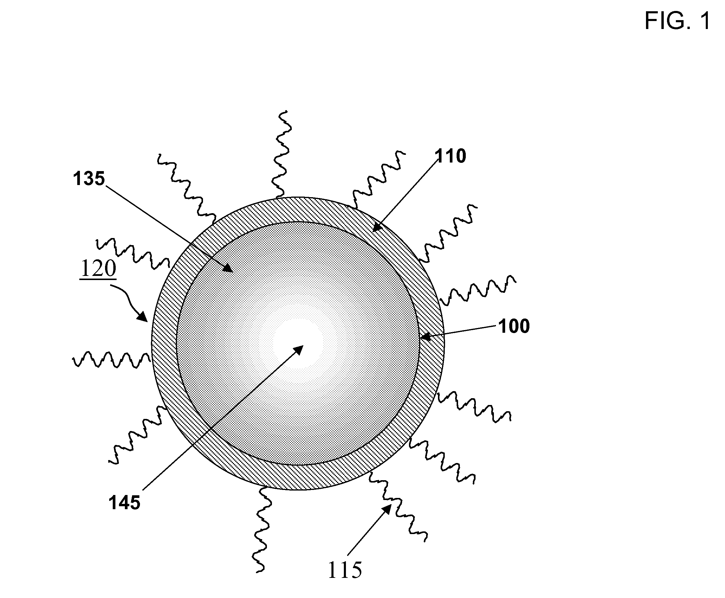
[0025]It is an advantage of the present invention that the non-blinking property of the ternary core / shell nanocrystals is not limited by type of solvent or type of surface ligands on the shell. This permits the nanocrystals to remain non-blinking in many environments and applications. It is an important feature of the invention that the ternary semiconductor cores have a gradient in alloy composition in order to achieve the non-blinking and short radiative lifetime properties. It is also an advantage that the ternary core / shell nanocrystals have much reduced radiative lifetimes compared to typical nanocrystals which enables enhanced quantum dot phosphor films, more efficient conventional LED devices, and single photon LED devices.
that the non-blinking property of the ternary core / shell nanocrystals is not limited by type of solvent or type of surface ligands on the shell. This permits the nanocrystals to remain non-blinking in many environments and applications. It is an important feature of the invention that the ternary semiconductor cores have a gradient in alloy composition in order to achieve the non-blinking and short radiative lifetime properties. It is also an advantage that the ternary core / shell nanocrystals have much reduced radiative lifetimes compared to typical nanocrystals which enables enhanced quantum dot phosphor films, more efficient conventional LED devices, and single photon LED devices.

Problems solved by technology

The blinking behavior of quantum dots, however, is generally considered an intrinsic limitation that is difficult to overcome.
Furthermore, blinking limits the use of colloidal quantum dots in luminescent applications such as single molecule LEDs.
The results of Hohng et al and Larson et al do not solve the intrinsic problems resulting in blinking dots, they only control the environment at the surface of the dots in order to mitigate the problem.
In addition to the problem of blinking, colloidal quantum dots suffer from increased radiative lifetimes as compared with their self-assembled counterparts.
The dominant ones are high manufacturing costs, difficulty in combining multi-color output from the same chip, and the need for high cost and rigid substrates.
In comparison to crystalline-based inorganic LEDs, OLEDs have much reduced brightness (mainly due to small carrier mobilities), shorter lifetimes, and require expensive encapsulation for device operation.
Because of problems, such as, aggregation of the quantum dots in the emitter layer, the efficiency of these devices was rather low in comparison with typical OLED devices.
The efficiency was even poorer when a neat film of quantum dots was used as the emitter layer (Hikmet et al., J. Appl. Phys. 93, 3509 (2003)).
The poor efficiency was attributed to the insulating nature of the quantum dot layer.
Regardless of any future improvements in efficiency, these hybrid devices still suffer from all of the drawbacks associated with pure OLED devices.
The resulting device had a poor external quantum efficiency of 0.001 to 0.01%.
These organic ligands are insulators and would result in poor electron and hole injection into the quantum dots.
In addition, the remainder of the structure is costly to manufacture, due to the usage of electron and hole semiconducting layers grown by high vacuum techniques, and the usage of sapphire substrates.
Despite these advantages, quantum dot phosphors have not been introduced into the marketplace due to some major shortcomings; such as, poor temperature stability and insufficient (10-30%) quantum yields for phosphor films with high quantum dot packing densities.
The disadvantage of this approach is that the resulting quantum dot phosphor films are unacceptably thick (1 mm), as compared to the desired thickness of 10 μm.
To date, optoelectronic devices or biological studies have not had colloidal quantum dots available that are inherently non-blinking or that have short radiative lifetimes. Previous methods to create non-blinking dots are application dependent and not universally applicable across the technical disciplines utilizing quantum dots.

Method used


Image

  • Device containing non-blinking quantum dots
  • Device containing non-blinking quantum dots
  • Device containing non-blinking quantum dots

Examples


example i-1

INVENTIVE EXAMPLE I-1

Preparation of the Inventive Ternary Core / Shell Non-Blinking Nanocrystals, CdxZn1-xSe / ZnSe

[0082]All synthetic routes were carried out using standard airless procedures with a dry box and a Schlenk line. The first step in creating the ternary cores was to form CdSe cores. Typically, 0.0755 g of TDPA (1-tetradecylphosphonic acid), 4 g of pre-degassed TOPO (trioctylphosphine oxide), and 2.5 g of HDA (hexadecylamine) were added in a three-neck flask. The mixture was degassed at 100° C. for half an hour. The stock solution of 1 M TOPSe was prepared by dissolving of 0.01 mol selenium in 10 ml TOP (trioctylphosphine). 1 ml of TOPSe was added to the flask and the mixture was heated to 300° C. The cadmium stock solution (0.06 g of CdAc2 in 3 ml TOP) was quickly injected under vigorous stirring resulting in nucleation of CdSe nanocrystals, after which time the temperature was set at 260° C. for further growth. After 5-10 min, the heating was removed and the flask was allo...

example i-2

INVENTIVE EXAMPLE I-2

Preparation of the Inventive Ternary Core / Shell Non-Blinking Nanocrystals, CdxZn1-xSe / ZnSeS

[0085]All synthetic routes were carried out using standard airless procedures with a dry box and a Schlenk line. The first step in creating the ternary cores was to form CdSe cores. In a three-neck flask, 0.2 mmol of CdO and 0.5 g of stearic acid were heated to 180° C. until the mixture went clear. Inside of a dry box, 3 ml of HDA and 6 ml of TOPO were added to the mixture. On a Schlenk line the mixture was heated to 310° C. under vigorous stirring, whereupon 1 ml of 1 M TOPSe was injected. The temperature was then lowered to 290-300° C. and stirred for an additional 10 minutes.

[0086]Next a ZnSe shell was formed on the CdSe cores. After cooling the core crude solution back to room temperature, it was reheated to 190° C. In a syringe was added 260 μl of 1 M diethylzinc in hexane, 260 μl of 1M TOPSe, and 2 ml of TOP. The contents of the syringe were then added to the CdSe co...


PUM


Abstract

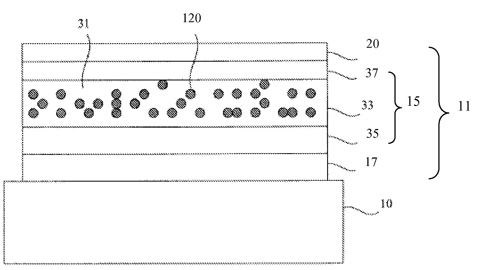
An optoelectronic device including two spaced apart electrodes; and at least one layer containing ternary core / shell nanocrystals disposed between the spaced electrodes and having ternary semiconductor cores containing a gradient in alloy composition and wherein the ternary core / shell nanocrystals exhibit single molecule non-blinking behavior characterized by on times greater than one minute or radiative lifetimes less than 10 ns.

Description

CROSS-REFERENCE TO RELATED APPLICATIONS[0001]Reference is made to commonly assigned U.S. patent application Ser. No. 11 / 226,622 filed Sep. 14, 2005, entitled “Quantum Dot Light Emitting Layer” by Keith B. Kahen; U.S. patent application Ser. No. 11 / 683,479 filed Mar. 8, 2007, entitled “Quantum Dot Light Emitting Device” by Keith B. Kahen; U.S. patent application Ser. No. 11 / 770,8334 filed Jun. 29, 2007, entitled “Light-Emitting Nanocomposite Particles” by Keith B. Kahen and U.S. patent application Ser. No. 11 / 926,538 filed Oct. 29, 2007, entitled “Making Colloidal Ternary Nanocrystals” by Keith B. Kahen et al, the disclosures of which are incorporated herein.STATEMENT REGARDING FEDERALLY-SPONSORED RESEARCH OR DEVELOPMENT[0002]This invention was made with Government support under Cooperative Agreement #DE-FC26-06NT42864 awarded by DOE. The Government has certain rights in this invention.FIELD OF THE INVENTION[0003]The present invention relates to applications using non-blinking nanocr...

Claims


Application Information

Patent Timeline
IPC IPC(8): G01N21/63H01J1/62
CPCC09K11/025C09K11/883
Inventor KAHEN, KEITH B.REN, XIAOFAN
Owner NANOCO TECH LTD
Learn More