
Spin transistor and method of manufacturing same

a technology of spin transistor and manufacturing method, which is applied in the manufacture of inductance/transformer/magnet, magnetic body, instruments, etc., can solve the problems of insufficient resistance, inability to solve, and difficulty in changing the resistance between the source and drain electrode by a sufficiently large ratio, so as to reduce the thickness of the semiconductor layer, and reduce the length of the channel.

Inactive Publication Date: 2009-03-05
TDK CORPARATION
View PDF9 Cites 18 Cited by
  • Summary
  • Abstract
  • Description
  • Claims
  • Application Information

AI Technical Summary

Benefits of technology

[0011]Such a problem can be alleviated by reducing the distance between the source and drain electrodes and thereby decreasing the channel length formed in the semiconductor layer. For reducing the distance between the source and drain electrodes, however, the conventional spin transistors have been limited in terms of fine processing techniques and thus have failed to solve the above-mentioned problem sufficiently.
[0031]The present invention can provide a spin transistor in which the resistance between the source and drain electrodes changes by a sufficiently large ratio between when the magnetization directions of the spin-polarized carrier injection layer and spin filter layer are parallel and antiparallel, and a method of manufacturing such a spin transistor.

Problems solved by technology

In the conventional spin transistors, however, the spin-polarized electrons injected into the semiconductor layer from the source electrode are spin-dispersed before reaching the drain electrode, so as to reduce the spin polarization ratio, which makes it difficult for the resistance between the source and drain electrodes to change by a sufficiently large ratio between when the magnetization directions of the spin-polarized electron injection layer and spin filter layer are parallel and antiparallel.
For reducing the distance between the source and drain electrodes, however, the conventional spin transistors have been limited in terms of fine processing techniques and thus have failed to solve the above-mentioned problem sufficiently.

Method used


Image

  • Spin transistor and method of manufacturing same
  • Spin transistor and method of manufacturing same
  • Spin transistor and method of manufacturing same

Examples


Embodiment Construction

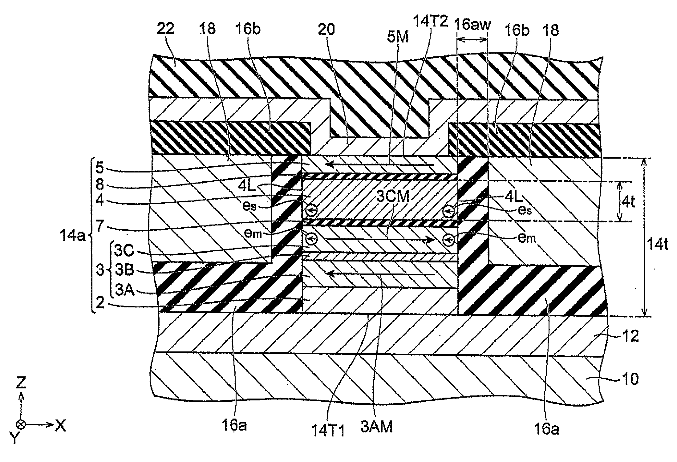
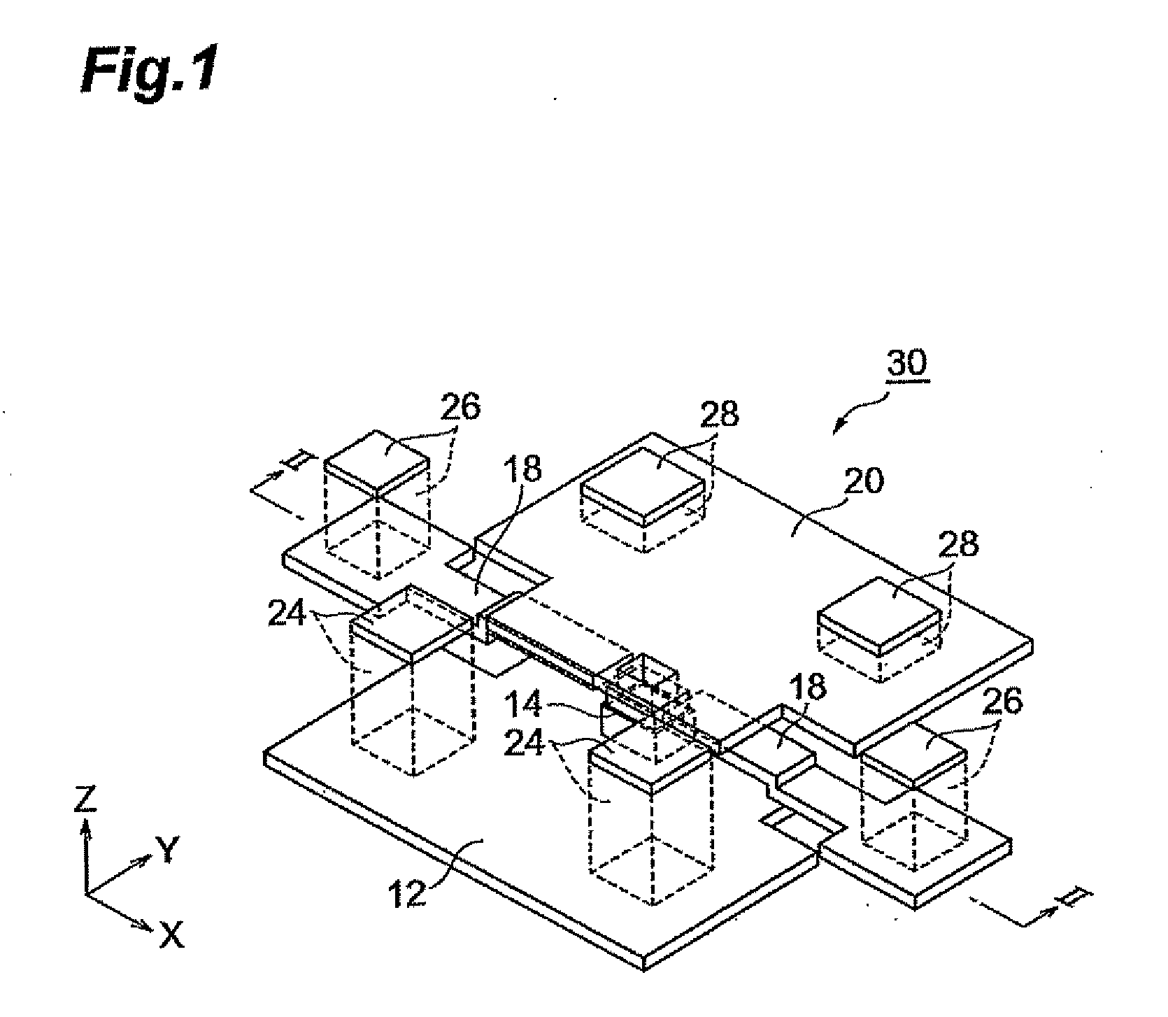
[0058]In the following, a spin transistor in accordance with an embodiment and a method of manufacturing the same will be explained in detail with reference to the accompanying drawings. In the drawings, the same constituents will be referred to with the same numerals or letters while omitting their overlapping descriptions. For easier viewing of the drawings, dimensional ratios within and among constituents in the drawings are arbitrary.

[0059]FIG. 1 is a perspective view of a spin transistor 30 in accordance with an embodiment, whereas FIG. 2 is a sectional view of the spin transistor 30 taken along the line II-II of FIG. 1. For easier viewing of the drawings, a silicon substrate 10, a gate insulating layer 16, and a protective layer 22 in FIG. 2 are not depicted in FIG. 1.

[0060]As shown in FIGS. 1 and 2, the spin transistor 30 comprises a magnetoresistive element 14 having a laminating direction along the Z axis, a source electrode layer 12 electrically connected to one end face 1...


PUM


Abstract

The spin transistor in accordance with the present invention comprises a magnetoresistive element having a fixed layer, a free layer, and a semiconductor layer provided between the fixed layer and free layer; a source electrode layer electrically connected to one end face in a laminating direction of the magnetoresistive element; a drain electrode layer electrically connected to the other end face in the laminating direction of the magnetoresistive element; and a gate electrode layer laterally adjacent to the semiconductor layer through a gate insulating layer provided on a side face of the semiconductor layer.

Description

BACKGROUND OF THE INVENTION[0001]1. Field of the Invention[0002]The present invention relates to a spin transistor and a method of manufacturing the same.[0003]2. Related Background Art[0004]Attention has recently been focused on studies about spin electronics. Spin transistors, which are transistors utilizing spins of electrons, have been expected to bring about new technological innovations. The spin transistors can be employed as storage devices having new structures (see Japanese Patent Application Laid-Open No, 2004-111904 and International Publication Pamphlet WO2004 / 079827) and multifunctional logic circuits (see International Publication Pamphlet WO2004 / 086625). They are made by magnetic material processes and thus may also be used as control devices for magnetic devices.[0005]In particular, FIG. 11 of Japanese Patent Application Laid-Open No. 2004-111904, FIG. 4 of U.S. Pat. No. 6,873,545B2, and FIG. 4 of U.S. Pat. No. 5,654,566 disclose spin transistors in which a nonmagne...

Claims


Application Information

Patent Timeline
IPC IPC(8): H01L29/00H01L21/00
CPCB82Y25/00G11C11/16H01F41/325H01F10/3272H01L29/66984H01F10/3254G11C11/161
Inventor KOGA, KEIJI
Owner TDK CORPARATION
Learn More