Method for production of silicon carbide layer, gallium nitride semiconductor device and silicon substrate
- Summary
- Abstract
- Description
- Claims
- Application Information
AI Technical Summary
Benefits of technology
Problems solved by technology
Method used
Image


Examples
Embodiment Construction
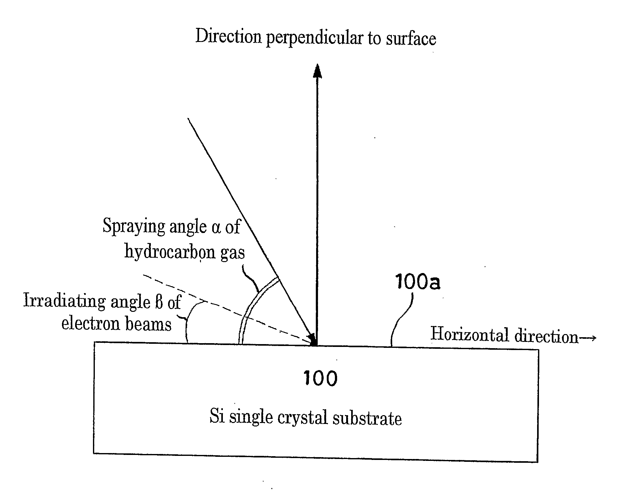
[0020]A cubic silicon carbide crystal layer, particularly 3C-silicon carbide layer (SiC layer) according to the Ramsdell notation, can be formed into a silicon substrate with a surface having various crystal planes (refer to “Electric Refractory Materials,” Marcel Decker, Inc., 2000, pp. 409-411). To form a 3C—SiC layer oriented in the [001] direction, it is advantageous that (001)-silicon with the (001) crystal plane as its surface be used as a substrate. To form a 3C—SiC layer oriented in the [111] direction, (111)-silicon with the (111) crystal plane as its surface is used as a substrate.
[0021]What is advantageously used to form a cubic silicon carbide crystal layer on the surface of a silicon substrate is gaseous hydrocarbon decomposed at low temperatures to produce carbon-containing fragments, which is acetylene (C2H2), for example. The easily decomposable aliphatic hydrocarbon gas is supplied into an MBE apparatus retained in high vacuum via flow rate control equipment capable...
PUM
 Abstract
Description
Claims
Application Information
 - R&D
- Intellectual Property
- Life Sciences
- Materials
- Tech Scout
- Unparalleled Data Quality
- Higher Quality Content
- 60% Fewer Hallucinations
Browse by: Latest US Patents, China's latest patents, Technical Efficacy Thesaurus, Application Domain, Technology Topic, Popular Technical Reports.
© 2025 PatSnap. All rights reserved.Legal|Privacy policy|Modern Slavery Act Transparency Statement|Sitemap|About US| Contact US: help@patsnap.com