Organic light emitting display device and manufacturing method thereof

Active Publication Date: 2009-01-15
SAMSUNG DISPLAY CO LTD +1
View PDF3 Cites 28 Cited by
  • Summary
  • Abstract
  • Description
  • Claims
  • Application Information

AI Technical Summary

Benefits of technology

[0009]The present invention is intended to provide a display device of high image quality in an organic light emitting display device using an organic light emitting element having an upper transparent electrode by decreasing the wiring resistance of the upper transparent electrode and lowering the unevenness of luminance in the display panel.
[0016]According to the invention, since the current supply line comprising a metal layer level with a driving layer or level with the layer of a lower electrode is connected with the upper transparent electrode to decrease the wiring resistance of the upper transparent electrode, unevenness of luminance in the display panel can be decreased, thus enabling display of high image quality. Further, since the transport layer constituting the organic light emitting element is formed over the entire display region of the display panel, and portions of the transport layer present at the connection portions are then removed, the number of precision masks to be used is decreased.
[0040]The electron injection layer referred to herein is used for improving the electron injection efficiency from the cathode to the electron transport layer. Specifically, lithium fluoride, magnesium fluoride, calcium fluoride, strontium fluoride, barium fluoride, magnesium oxide, and aluminum oxide are preferred. They are not restricted to the materials, but two or more of the materials may be used in combination.
[0043]The protective layer referred to herein is formed on the upper electrode and is intended for preventing atmospheric H2O, O2 from intruding into the upper electrode or the organic layer below.
[0048]In the active matrix organic light emitting display device, a driving element constituted with 2 to 4 switching elements of thin film transistors and capacitors is connected to the organic EL (light emitting) element constituting each of the pixels, and lighting up during a full period of one frame is possible. Accordingly, it is not necessary to increase the luminance and the life of the organic light emitting element can be made longer.

Problems solved by technology

In the case of using a highly-resistive transparent conductive film for the upper transparent electrode, unevenness in applied voltages occurs between a pixel comprising an organic light emitting element at the periphery of the display panel near the power source and a pixel comprising an organic light emitting element at the central portion of the display panel due to the wiring resistance caused of the upper transparent electrode, which, as a result, generates unevenness of luminance.
Accordingly, for the entire organic layer, a transport layer as well as the light emitting layer has also to be formed by using a precision mask, which results in a problem of lowering the mass productivity.

Method used


Image

  • Organic light emitting display device and manufacturing method thereof
  • Organic light emitting display device and manufacturing method thereof
  • Organic light emitting display device and manufacturing method thereof

Examples


first embodiment

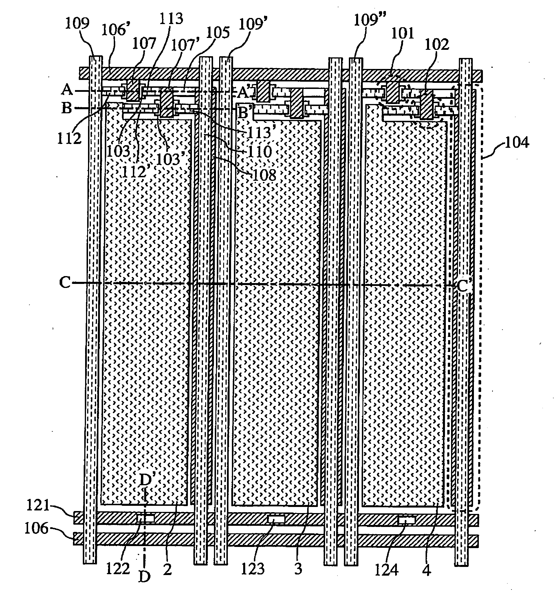
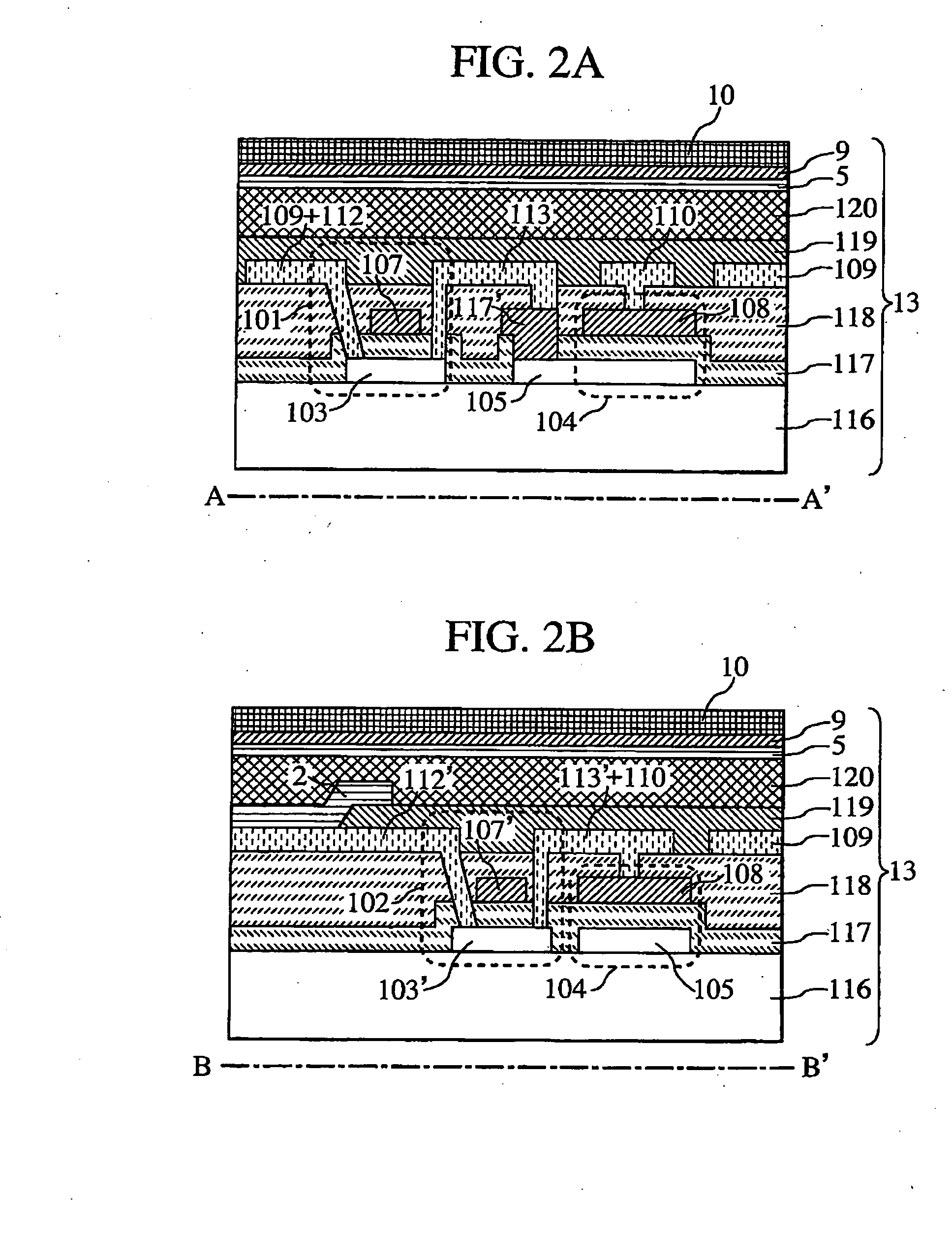
[0088]A preferred embodiment of an organic light emitting display device according to the invention is to be described with reference to the drawings. FIG. 1 is a plan view of a pixel of the organic light emitting display device. FIG. 2A is a cross sectional view taken along the line A-A′ shown in FIG. 1, and FIG. 2B is a cross sectional view taken along the line B-B′ shown in FIG. 1. FIG. 3 is a cross sectional view taken along the line C-C′ shown in FIG. 1. FIG. 4 is a cross sectional view taken along the line D-D′ shown in FIG. 1.

[0089]In FIG. 1 to FIG. 4, above a glass substrate 116, a plurality of gate lines 106 are disposed at predetermined intervals, and data lines 109 for transmitting image information are also disposed at predetermined intervals in the direction intersecting each of the gate lines. That is, the gate lines 106 and the data lines 109 are arranged in matrix, and regions surrounded by gate lines 106 and the data lines 109 each constitute a display region for on...

second embodiment

[0118]Next, a second embodiment of the organic light emitting display device according to the invention is to be described. FIG. 5 is a plan view of a pixel of the organic light emitting display device, and FIG. 6 is a cross sectional view taken along the line D-D′ shown in FIG. 5. This embodiment is characterized in that a second current supply line 131 and the lower electrodes 2 to 4 are formed in the same layer. With this configuration, step disconnection of the upper transparent electrode 10 at the periphery of the contact holes can be suppressed.

[0119]Specifically, the method of forming the first transistor 101, the second transistor 102, the capacitor 104, the data line 109, the gate line 106, the first current supply line 110, the gate insulating film 117, the first interlayer insulating film 118, the second interlayer insulating film 119 and the lower-electrodes 2 to 4 above the glass substrate 116 is identical with that of the first embodiment.

[0120]As shown in FIG. 6, the ...

third embodiment

[0126]Next, a third embodiment of the organic light emitting display device according to the invention is to be described. FIG. 7 is a plan view of a pixel of the organic light emitting display device, and FIG. 8 is a cross sectional view taken along the line D-D′ shown in FIG. 7. In this embodiment, a second current supply line 141 formed in the same layer as those of the gate line 106 and the upper transparent electrode 10 are connected electrically via a metal layer level with the lower-electrodes 2 to 4. Therefore, step disconnection of the upper transparent electrode 10 near the contact hole is suppressed.

[0127]Specifically, the first transistor 101, the second transistor 102, the capacitor 104, the data line 109, the gate line 106, the second current supply line 141, the first current supply line 110, the gate insulating film 117, the first interlayer insulating film 118, and the second interlayer insulating film 119 are formed above the glass substrate 116. Manufacturing cond...


PUM


Abstract

The present invention provides an organic light emitting device in which an upper transparent electrode 10 of an organic light emitting device 2 is connected electrically at a contact hole portion 122 to a current supply line 121 disposed in the same layer as that of and extending in parallel with a gate line 106. That is, a hole transport layer 5 and an electron transport layer 9 of the organic light emitting device 2 are formed over the entire display region, and then a contact hole portion 122 is removed to electrically connect the current supply line 121 and the upper transparent electrode 10, thereby decreasing unevenness of luminance due to wiring resistance of the upper transparent electrode.

Description

BACKGROUND OF THE INVENTION[0001]1. Field of the Invention[0002]The present invention relates to decrease in the resistance of an upper transparent electrode of a self-emitting organic electroluminescent device.[0003]2. Description of the Related Art[0004]A self-emitting organic electroluminescent element (hereinafter referred to as an “organic light emitting element”) is expected as an illumination device for a thin-screen display device and a liquid crystal display device.[0005]An organic light emitting display device includes a plurality of organic light emitting elements constituting pixels on a substrate and a driving layer for driving the organic light emitting elements. The organic light emitting element has a structure in which a plurality of organic layers are put between a lower electrode and an upper transparent electrode. The plurality of organic layers include at least a transport layer for transporting electron holes, a transport layer for transporting electrons and a ...

Claims


Application Information

Patent Timeline
IPC IPC(8): H01L51/52H01J9/02
CPCH01L27/3276H01L2251/5315H01L51/5212H10K59/131H10K2102/3026H10K59/80516H10K59/1315H10K50/814
Inventor ISHIHARA, SHINGOMATSUZAKI, EIJI
Owner SAMSUNG DISPLAY CO LTD
Why Eureka
Try Eureka