
Oled Having Stacked Organic Light-Emitting Units

a light-emitting unit and organic technology, applied in the field of stacking organic light-emitting devices, can solve the problems of deteriorating critical characteristics of the device such as light-emitting efficiency, difficult to inject electrons from the cathode to the light-emitting layer, and large increase in the operational voltage of the organic light-emitting devices, etc., to achieve high device efficiency and availability, and simplify the preparation process of the device.

Active Publication Date: 2009-01-08
LG DISPLAY CO LTD
View PDF108 Cites 100 Cited by
  • Summary
  • Abstract
  • Description
  • Claims
  • Application Information

AI Technical Summary

Benefits of technology

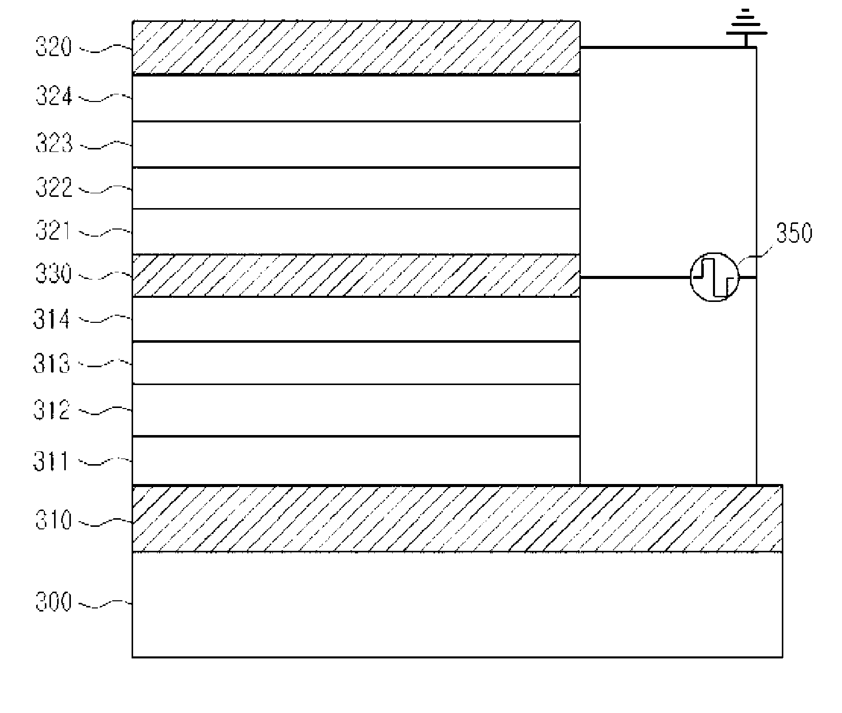
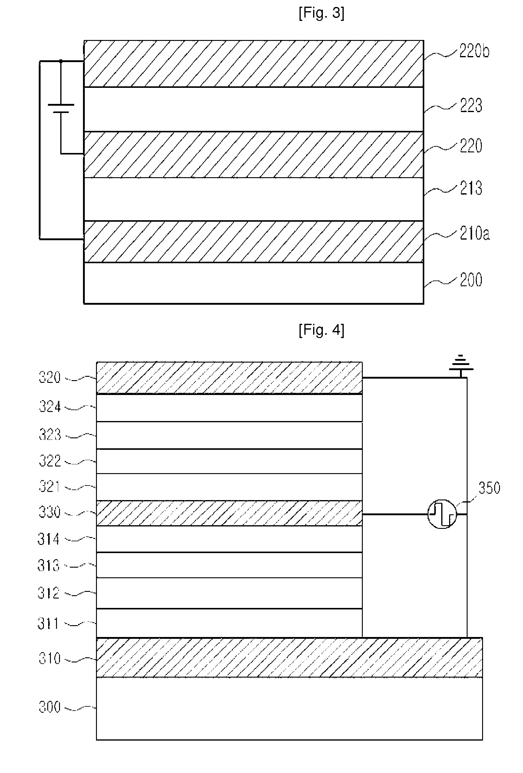
[0016]It is an advantage of the stacked organic light emitting device according to the present invention that it is capable of color temperature control through the partial color control by individually operating each of the stacked light emitting units, and it is capable of establishment of various display devices by alternately operating the stacked light emitting units. Since the organic light emitting device according to the present invention comprises an n-type organic material layer and a p-type organic material layer, wherein a combination thereof lowers the electrical barrier against hole injection and hole discharge, and forms an NP junction, it provides a high device efficiency and availability of various materials for the electrode materials, thus it giving an effect of simplifying the preparation process for the device.

Problems solved by technology

Consequently, when it is used to form a cathode electrode, it is not easy to inject electrons from the cathode to the light emitting layer.
From this, there occur some problems that the operational voltage of the organic light emitting device is greatly increased, and that critical characteristics as the device such as light emitting efficiency is deteriorated.
Accordingly, it has some limitation on the use of the transparent electrode, which is used as an anode electrode, as a common electrode acting as both of an anode electrode and a cathode electrode.
However, since the hole injecting layer should be selected taking into consideration not only the Fermi energy level of the anode electrode, but also the HOMO energy level of the hole transporting layer or the light emitting layer, there is some limitation on selection of the materials for the hole injecting layer.
Accordingly, even in the case of using the materials used for a cathode such as a Mg:Ag alloy layer as a common electrode, light emitting characteristics are inevitably limited.
This SOLED allows color temperature calibration of each unit of the light emitting layers, but color temperature control needs a very complicated electrode structure.
Further, this SOLED has a drawback that the preparation process is complicated, for example, due to formation of a Mg:Ag / ITO double layer having limited transparency.
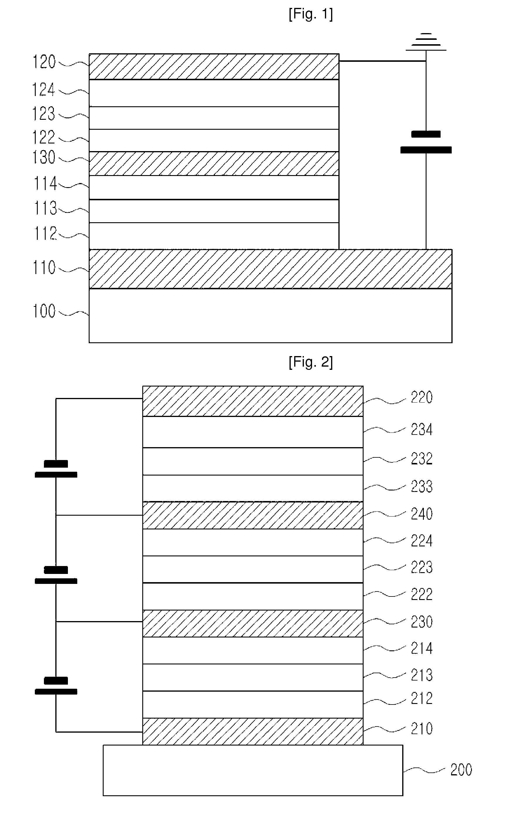
However, in such the stacked organic light emitting device, two light emitting units on the right side and the left side of the intermediate conductive layer (220) are formed in an inverting structure and a non-inverting structure, and accordingly, it is substantially only configured to make the same currents to be applied to a unit device simultaneously, which does not allow color temperature calibration.

Method used


Image

  • Oled Having Stacked Organic Light-Emitting Units
  • Oled Having Stacked Organic Light-Emitting Units
  • Oled Having Stacked Organic Light-Emitting Units

Examples


example 1

Double Stacked Organic Light Emitting Device

[0113]On a washed glass substrate, indium zinc oxide (IZO) was coated to a thicknesses of 1000 Å by vacuum deposition using a sputtering deposition apparatus, and on the formed conductive layer, HAT having the following structure was coated to a thicknesses of 500 Å by thermal vacuum deposition to form a transparent anode comprising the IZO and HAT n-type organic material layers.

[0114]Then, on the HAT n-type organic material layer, 4,4′-bis[N-(1-naphthyl)-N-phenylamino]biphenyl (NPB) was coated to a thicknesses of 400 Å by vacuum deposition to form a p-type hole transporting layer. On the p-type hole transporting layer, a blue host material represented by the following formula 2-1 was doped with a blue dopant material represented by the following formula 2-2 to a concentration of 2%, and coated to a thicknesses of about 300 Å by vacuum deposition to form a light emitting layer. Then, on the light emitting layer, the following imidazole com...


PUM


Abstract

The present invention provides a stacked organic light emitting device, comprising a first conductive layer, at least one intermediate conductive layer and a second conductive layer, and light emitting units disposed between the conductive layers, wherein at least two non-neighboring conductive layers among the conductive layers are conductive layers belonging to Group 1 such that they are electrically connected with each other to a common potential; at least one non-neighboring conductive layer among the conductive layers which are not electrically connected with the conductive layers belonging to Group 1 to a common potential are conductive layers belonging to Group 2 such that they are electrically connected with each other to a common potential; and the conductive layers belonging to Group 1 and the conductive layers belonging to Group 2 are connected with each other via a voltage regulator for alternately applying a positive voltage and a negative voltage.

Description

TECHNICAL FIELD[0001]The present invention relates to a stacked organic light emitting device (OLED). This application claims priority benefits from Korean Patent Application No. 10-2006-0005200, filed on Jan. 18, 2006, the entire contents of which are fully incorporated herein by reference.BACKGROUND ART[0002]An organic light emitting device usually comprises two electrodes, and an organic material layer interposed therebetween. The organic light emitting device can further comprise an electron- or hole-injecting layer, or an electron- or hole-transporting layer to improve the performances.[0003]Recently, a stacked organic light emitting device which can enhance the light emitting efficiency per unit area by interposing an organic light emitting layer in the pixel regions of the organic light emitting device has been developed.[0004]FIG. 1 illustrates a cross-section of the conventional stacked organic light emitting device. The device shown in FIG. 1 has a stacked structure in whi...

Claims


Application Information

Patent Timeline
Patent Type & Authority Applications(United States)
IPC IPC(8): H05B41/16
CPCH01L27/3209H01L2251/564H01L51/5278H10K59/32H10K50/19H10K71/841H05B33/26C09K11/06
Inventor KANG, MIN-SOONOH, JEOUNG-KWENLEE, JUNG-HYOUNG
Owner LG DISPLAY CO LTD
Learn More