Method of manufacturing nonvolatile memory device using conductive organic polymer having nanocrystals embedded therein

a technology of conductive organic polymer and nonvolatile memory, which is applied in the direction of solid-state devices, nanoinformatics, instruments, etc., can solve the problems of low data processing speed of flash memory, large amount of power, and large increase in voltage used therein, so as to achieve high integration density, high operating speed, and low power consumption

Inactive Publication Date: 2008-12-11
SAMSUNG ELECTRONICS CO LTD
View PDF10 Cites 2 Cited by
  • Summary
  • Abstract
  • Description
  • Claims
  • Application Information

AI Technical Summary

Benefits of technology

[0011]Aspects of the present invention provide a conductive organic nonvolatile memory device which causes no data loss even when being powered off, consumes less power, contributes high integration density and which provides high operating speed, and a method of manufacturing the conductive organic nonvolatile memory device.
[0012]Aspects of the present invention also provide a nonvolatile memory device and a method of manufacturing the same, in which the bistable conduction property of an organic material may be maintained by establishing optimum processing conditions and the thermal stability of a nonvolatile memory device may also be maintained by using a conductive organic material having the properties of a polymer.

Problems solved by technology

However, a DRAM needs to continuously charge a capacitor and generally consumes a considerable amount of power because of a high probability of data loss caused by a leakage current.
However, a flash memory may cause a considerable increase in voltage used therein due to the use of F-N tunneling.
Further, the data processing speed of a flash memory is generally low since a flash memory reads or writes data in a predetermined order.
In order to provide such conventional memory devices, a minimum of hundreds to thousands of processes may need to be performed, which reduces the manufacturing yield.
In addition, dozens to thousands of patterns including gates, sources and drains may need to be formed, which makes it difficult to increase the integration density of memory devices.
The use of conductive organic materials has not yet been widespread in manufacturing memory devices.
A drawback to their use is that it is difficult to determine optimum processing conditions to manufacture memory devices using conductive organic materials.
Further, low-molecular weight conductive organic materials, which have been widely used to manufacture conventional memory devices, are vulnerable to heat and are thus often likely to result in breakdown of the properties of memory devices, especially when the memory devices are operated at a temperature of above 200° C.

Method used


Image

  • Method of manufacturing nonvolatile memory device using conductive organic polymer having nanocrystals embedded therein
  • Method of manufacturing nonvolatile memory device using conductive organic polymer having nanocrystals embedded therein
  • Method of manufacturing nonvolatile memory device using conductive organic polymer having nanocrystals embedded therein

Examples


Embodiment Construction

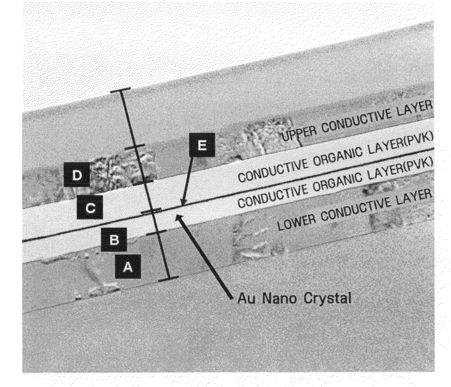
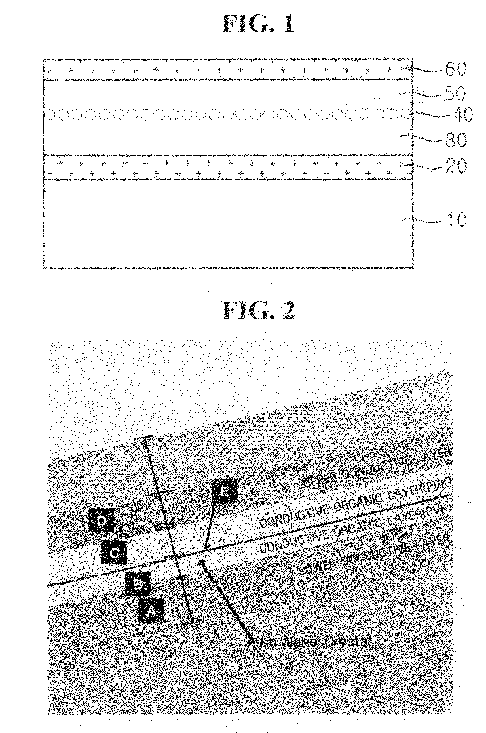
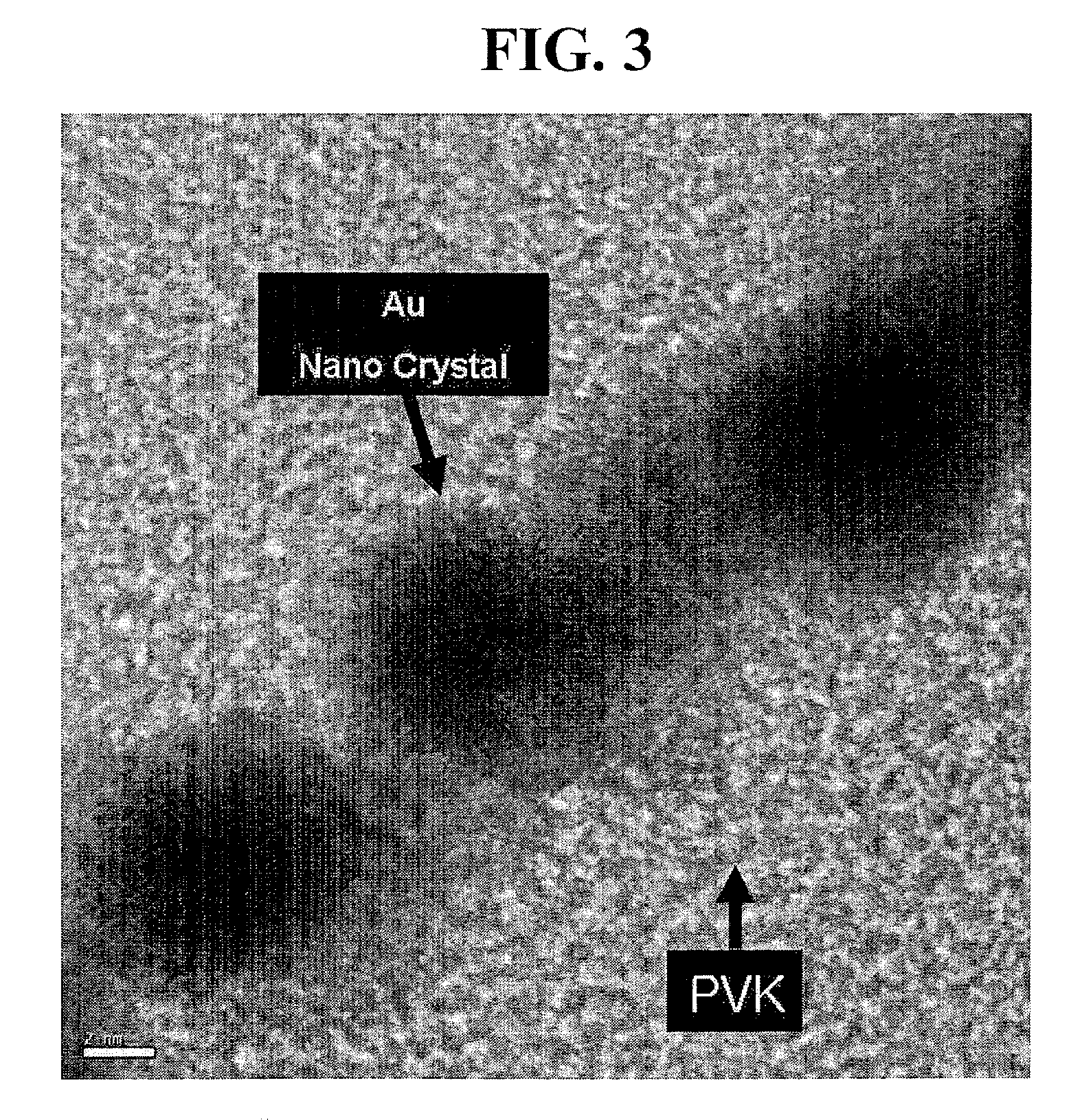
[0035]The present invention will now be described more fully with reference to the accompanying drawings, in which exemplary embodiments of the invention are shown. The invention may, however, be embodied in many different forms and should not be construed as being limited to the embodiments set forth herein. Rather, these embodiments are provided so that this disclosure will be thorough and complete, and will fully convey the concept of the invention to those skilled in the art.

[0036]It will be understood that when an element is referred to as being “connected” or “coupled” to another element, it can be directly connected or coupled to the other element or intervening elements may be present. In contrast, when an element is referred to as being “directly connected” or “directly coupled” to another element, there are no intervening elements present. Like numbers refer to like elements throughout. As used herein the term “and / or” includes any and all combinations of one or more of th...


PUM

PropertyMeasurementUnit
temperatureaaaaaaaaaa

Abstract

The method of manufacturing a nonvolatile memory device includes forming a lower conductive layer on a substrate; forming a first conductive organic layer on the substrate using spin coating; forming a metal layer for forming nanocrystals on the first conductive organic layer, the metal layer partially overlapping the first conductive organic layer; forming a second conductive organic layer on the first conductive organic layer using spin coating; transforming the metal layer into nanocrystals by curing; and forming an upper conductive layer on the second conductive organic layer, the upper conductive layer partially overlapping the nanocrystals. The conductive organic polymer may be poly-N-vinylcarbazole (PVK) or polystyrene (PS).

Description

CROSS-REFERENCE TO RELATED APPLICATION[0001]This application claims priority from Korean Patent Application Nos. 10-2007-0040521 and 10-2007-0040520 each filed on Apr. 25, 2007 in the Korean Intellectual Property Office, the disclosures of which are incorporated herein by reference in their entireties.BACKGROUND OF THE INVENTION[0002]The present invention relates to a nonvolatile memory device and a method of manufacturing the nonvolatile memory device, and more particularly, to a nonvolatile memory device using a conductive organic material having metallic nanocrystals that can provide two different conductive states at the same voltage, and a method of manufacturing the nonvolatile memory device.[0003]Memory devices are largely classified into volatile memory devices such as dynamic random access memory (DRAM) devices and nonvolatile memory devices such as flash memory devices.[0004]A DRAM forms a channel between source and drain terminals by adjusting the channel width under a ga...

Claims


Application Information

Patent Timeline
Patent Type & Authority Applications(United States)
IPC IPC(8): H01L51/30H10K99/00
CPCB82Y10/00G11C13/0014G11C13/0016G11C2211/5614H01L51/0042H01L51/0575H01L51/0591H10K85/146H10K10/20H10K10/50
Inventor PARK, JEA-GUNLEE, GON-SUBHAN, BYEONG-ILLEE, JONG-DAE
Owner SAMSUNG ELECTRONICS CO LTD
Why Eureka
Try Eureka