
Photoelectric conversion element and solar cell

Active Publication Date: 2008-12-04
KONICA MINOLTA BUSINESS TECH INC
View PDF1 Cites 34 Cited by
  • Summary
  • Abstract
  • Description
  • Claims
  • Application Information

AI Technical Summary

Benefits of technology

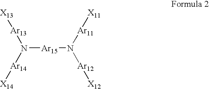
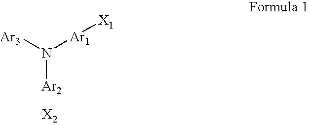
[0055]When the plural kinds of the compound represented by Formulas 1 or 2 or a combination with another sensitizing dye are used, it is allowed that a solution of mixture of various dyes is prepared and used or that solutions of each of the compounds are separately prepared and the semiconductor layer is successively immersed therein. In the case of that the solutions of each of the compounds or another sensitizing dye are separately prepared and the semiconductor layer is successively immersed in these solutions, the effect of the invention can be obtained even when the immersion is carried out in any order. Moreover, the transducer can be prepared by using a mixture of the semiconductor particles on each of which the compounds or another dye are individually adsorbed.
[0056]The adsorbing treatment may be applied to the semiconductor in a particle state or a layer state formed on a substrate. The solution of the compound to be used for the adsorption treatment may be used at room temperature or in a heated state at a temperature within the range in which the compound is not decomposed and the solution is not boiled. The adsorption of the dye may be performed after coating of the fine particles of the semiconductor as later-mentioned. The adsorption of the compound may also be performed by simultaneously coating the fine particles of the semiconductor and the dye. The dye not adsorbed to the semiconductor can be removed by washing.
[0057]The sensitization of the semiconductor layer is carried out by adding the compound represented by Formulas 1 or 2, and the detail of the sensitization treatment is described in the later description relating to the photoelectric conversion element.
[0058]In the case of the semiconductor layer has a semiconductor thin layer having high porosity, it is preferred that the treatment by the dye or the sensitizing dye (sensitizing treatment for the semiconductor layer) is completed before the adsorption of water caused by water or vapor thereof in the pores of the surface and interior of the semiconductor thin layer.
[0059]The semiconductor layer may be treated by an organic base. As the organic base, diphenylamine, triphenylamine, pyridine, 4-t-butylpyridine, polyvinylpyridine, quinoline, piperidine and amidine are cited. Among them, pyridine, 4-t-butylpyridine and polyvinylpyridine are preferred.
[0060]When the above organic base is a liquid, the compound is used itself and when the amine compound is solid, a solution of it dissolved in an organic solvent is prepared, and the surface treatment can be performed by immersing the semiconductor layer into the above liquid amine or the amine solution.

Problems solved by technology

However, the solar cells, for example, the silicone type have drawbacks such as that extremely high purity is required so that complicated process including many steps is necessary and the production cost is raised.
However, there is doubt as to supply of ruthenium when such the solar cells are practically used since ruthenium is limited resource.
Moreover, ruthenium is high in the coast and has a problem of aging stability.
However, the absorption peak of the solution of such the dye is not more than 500 nm and a problem that the absorption at the long wavelengths side is weak is left.

Method used


Image

  • Photoelectric conversion element and solar cell
  • Photoelectric conversion element and solar cell
  • Photoelectric conversion element and solar cell

Examples


example 1

[0103]Preparation of Photoelectric Conversion Element 1

[0104]Titanium oxide paste having a particle size of 18 nm was coated by a screen printing method on a glass substrate given electroconductivity by fluorine-doped tin oxide (FTO). The paste was dried by heating at 60° C. for 10 minutes and burned at 500° C. for 30 minutes to obtain a titanium oxide thin layer having a thickness of 5 μm.

[0105]Dye 1 was dissolved in ethanol to prepare a solution having a concentration of 3×10⁻⁴ moles / l. The FTO glass substrate on which the titanium oxide paste was coated and burned was immersed in the above solution for 16 hours at room temperature for performing dye adsorption to prepare a semiconductor electrode.

[0106]As the charge transfer layer (electrolysis solution), a. 3-methoxypropionitrile solution containing 0.6 g / l of 1,2-dimethyl-3-propylimidazolium iodide, 0.1 moles / l of lithium iodide, 0.05 moles / l of iodine and 0.5 moles / l of 4-(t-butyl)pyridine was used. A platinum plate was used f...


PUM

PropertyMeasurementUnit
Acidityaaaaaaaaaa
Photoelectricityaaaaaaaaaa
Semiconductor propertiesaaaaaaaaaa

Abstract

A photoelectric conversion element having a pair of electrodes, and a semiconductor layer comprising a semiconductor carrying a dye and an electrolyte layer is disclosed. The dye is represented by Formulas 1 or 2;in Formula 1, Ar1 and Ar2 are each an arylene or heterocyclic group, or a composite group of an arylene group and a heterocyclic group, each of which may have a substituent, Ar3 is an aryl or heterocyclic group or a composite group of an arylene group and a heterocyclic group, each of which may have a substituent, Ar1, Ar2 and Ar3 may form a ring by bonding with each other, X1 and X2 are each a straight chain residue having an acidic group which may have a mono-valent substituent, and one to eight saturated or unsaturated aliphatic hydrocarbon group having 5 to 30 carbon atoms are contained among Ar1, Ar2 and Ar3;in the formula, Ar11, Ar12, Ar13, Ar14 and Ar15 are each an arylene or heterocyclic group, or a composite group of an arylene group and a heterocyclic group, each of which may have a substituent, Ar11, Ar12, Ar13, Ar14 and Ar15 may form a ring by bonding with together, at least two of X11, X12, X13 and X14 are each an alkyl or alkenyl group having an acidic group which may have a mono-valent substituent and the remainders are each a hydrogen atom, and one to eight saturated or unsaturated aliphatic hydrocarbon group having 5 to 30 carbon atoms are contained among Ar11, Ar12, Ar13, Ar14 and Ar15.

Description

[0001]This application is based on Japanese Patent Application No. 2007-144881 filed on May 31, 2007, the entire content of which is hereby incorporated by reference.TECHNICAL FIELD[0002]The present invention relates to a dye-sensitized type photoelectric conversion element and a solar cell constituted by using the photoelectric conversion element.TECHNICAL BACKGROUND[0003]Recently, application of solar light is energetically investigated, which is infinity and generate no noxious substance. As the means practically used at the present time for utilizing the clean energy source of solar light, inorganic solar cells such as single crystal silicone for domestic use, polycrystal silicone, amorphous silicone, cadmium telluride and indium copper selenide are cited.[0004]However, the solar cells, for example, the silicone type have drawbacks such as that extremely high purity is required so that complicated process including many steps is necessary and the production cost is raised.[0005]...

Claims


Application Information

Patent Timeline
IPC IPC(8): H01L51/46
CPCH01G9/2004H01G9/2013H01G9/2031H01G9/2059H01L51/0053H01L51/0059H01L51/006H01L51/0061H01L51/0068H01L51/0071H01L51/0072H01L51/4226H01L2251/306Y02E10/542Y02E10/549H10K85/621H10K85/655H10K85/636H10K85/633H10K85/631H10K85/657H10K85/6572H10K2102/102H01G9/20H10K30/151
Inventor NISHIMURA, KAZUKUNIITAMI, AKIHIKOMOCHIZUKI, FUMITAKAMIWA, HIDEYAKAWASAKI, HIDEKAZU
Owner KONICA MINOLTA BUSINESS TECH INC
Learn More