Semiconductor laser diode
a laser diode and semiconductor technology, applied in lasers, lasers, semiconductor lasers, etc., can solve problems such as achieve the effects of reducing light emission efficiency, reducing polarization in quantum wells, and increasing light emission efficiency
- Summary
- Abstract
- Description
- Claims
- Application Information
AI Technical Summary
Benefits of technology
Problems solved by technology
Method used
Image

Examples
first embodiment
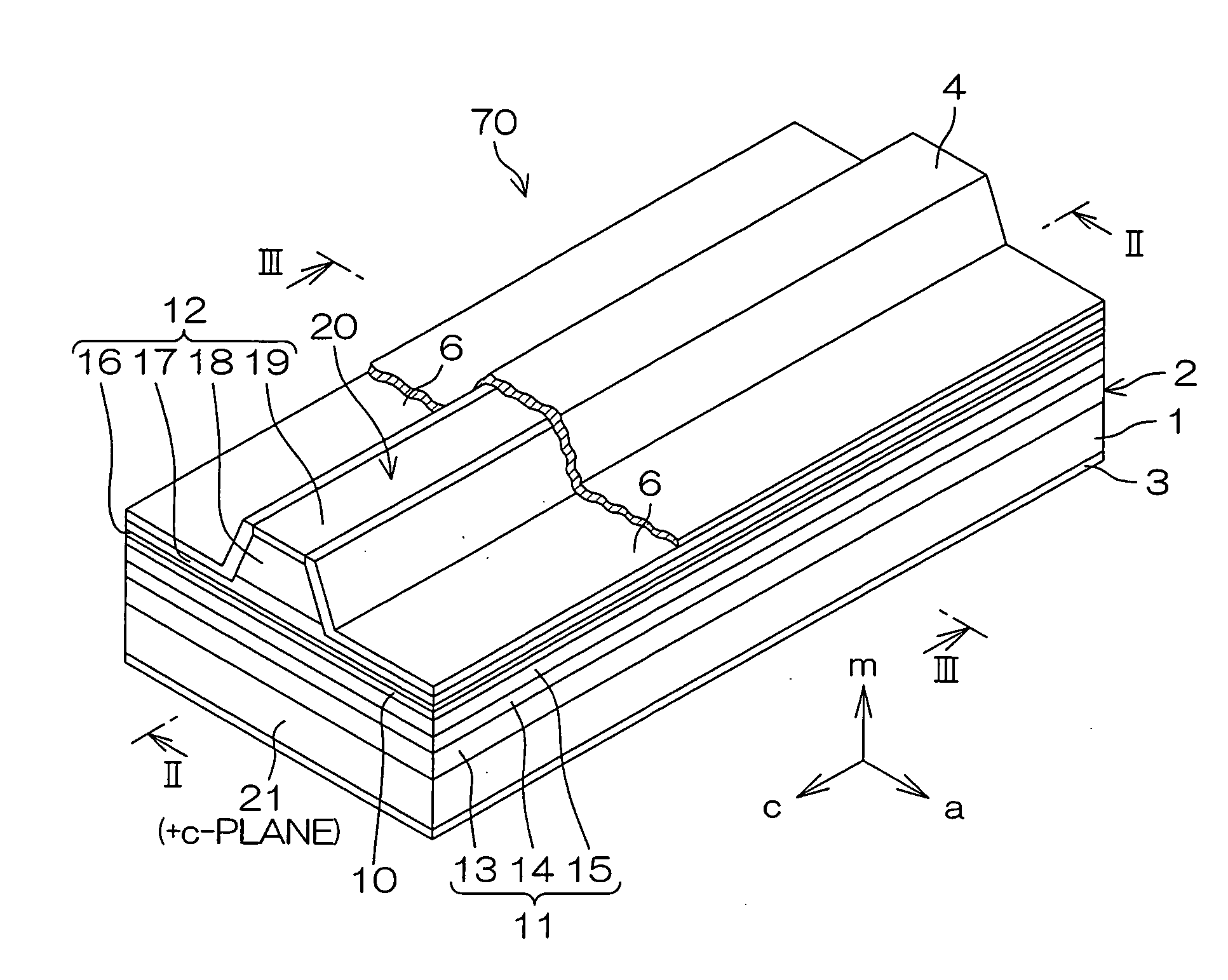
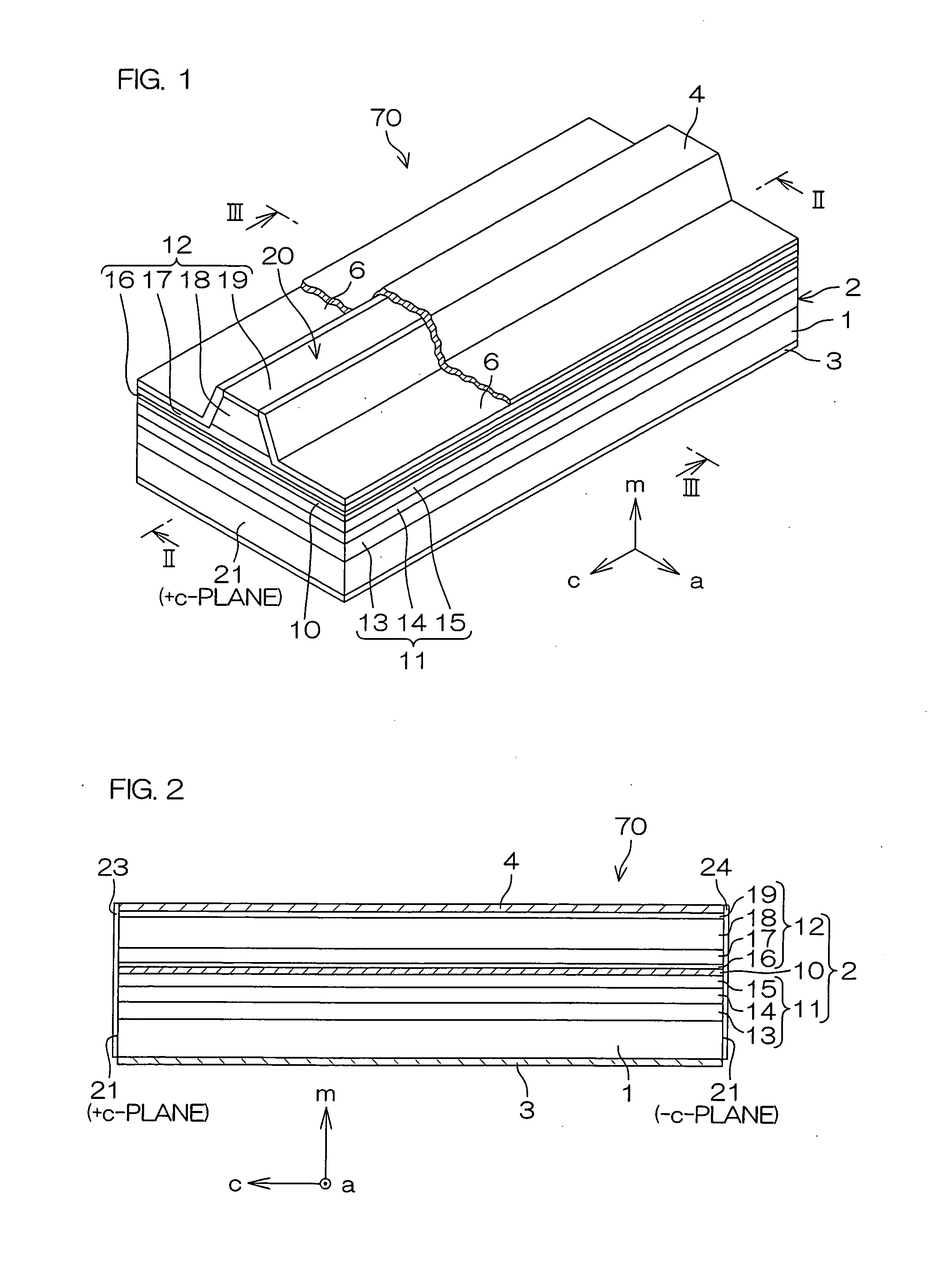
[0058]FIG. 1 is a perspective view for explaining the construction of a semiconductor laser diode according to the present invention.
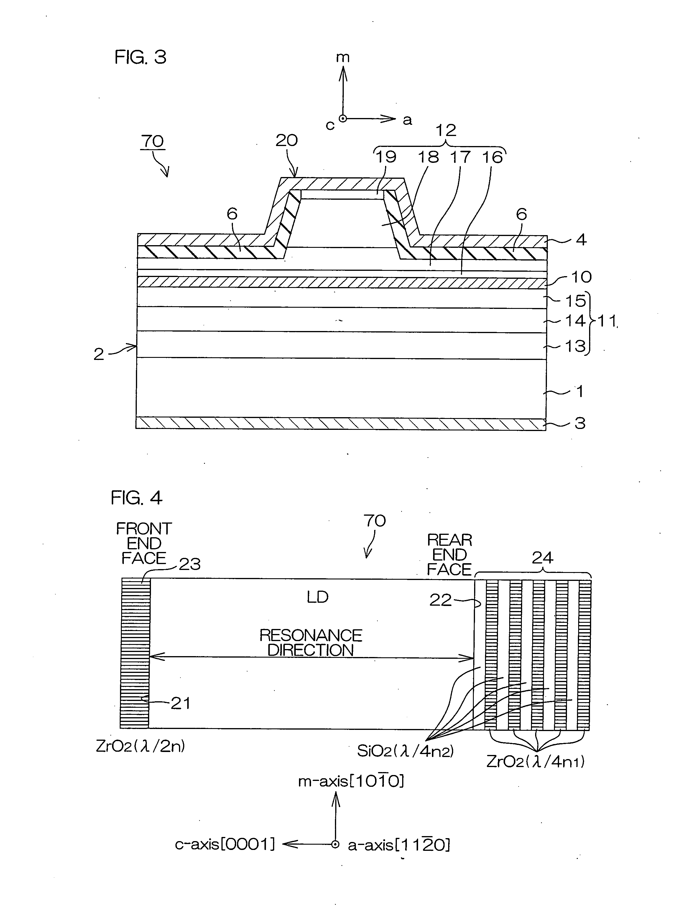
[0059]FIG. 2 is a longitudinal sectional view taken along a line II-II in FIG. 1, and FIG. 3 is a transverse sectional view taken along a line III-III in FIG. 1.
[0060]The semiconductor laser diode 70 is of a Fabry-Perot type, which includes a substrate 1, a Group III nitride semiconductor layered structure 2 formed on the substrate 1 through crystal growth, an n-side electrode 3 provided in contact with a rear surface of the substrate 1 (a surface of the substrate 1 opposite from the Group III nitride semiconductor layered structure 2), and a p-side electrode 4 provided in contact with a front surface of the Group III nitride semiconductor layered structure 2.
[0061]In this embodiment, the substrate 1 is a GaN monocrystalline substrate. The substrate 1 has a major surface defined by an m-plane, and the Group III nitride semiconductor layered structure 2...
second embodiment
[0121]FIG. 8 is a perspective view showing the construction of a semiconductor laser diode according to the present invention, and FIG. 9 is a longitudinal sectional view taken along a sectional line IX-IX in FIG. 8. In FIGS. 8 and 9, portions corresponding to those shown in FIGS. 1 to 3 will be denoted by the same reference characters as in FIGS. 1 to 3.
[0122]In the semiconductor laser diode 80 according to this embodiment, the ridge stripe 20 extends parallel to the a-axis, so that the resonator end faces 21, 22 are each defined by the a-plane. These resonator end faces 21, 22 are each a cleaved surface formed by cleavage.
[0123]Layering defects are liable to occur parallel to the c-plane when the Group III nitride semiconductor layered structure 2 is epitaxially grown. In the arrangement according to the first embodiment, therefore, the layering defects are liable to cross the optical waveguide. In this embodiment, on the contrary, the stripe extending direction is parallel to the...
third embodiment
[0124]FIG. 10 is a perspective view for explaining the construction of a semiconductor laser diode according to the present invention. In FIG. 10, portions corresponding to those shown in FIG. 1 will be denoted by the same reference characters as in FIG. 1.
[0125]In the semiconductor laser diode 90 according to this embodiment, the Group III nitride semiconductor layered structure 2 includes an In-containing layer having a biaxial stress, i.e., an n-type InGaN layer 26 (for example, having a thickness of 0.1 μm and an n-type impurity concentration of 1×1018 cm−3), provided between the substrate 1 and the n-type GaN contact layer 13. The provision of the n-type InGaN layer 26 suppresses cracking occurring parallel to the c-plane in the Group III nitride semiconductor layered structure 2 due to reduction in the biaxial stress and the lattice constant.
[0126]Where a GaN monocrystalline substrate 1 having a major plane defined by the m-plane is used as the substrate 1 and the Group III ni...
PUM
 Abstract
Description
Claims
Application Information
 - R&D
- Intellectual Property
- Life Sciences
- Materials
- Tech Scout
- Unparalleled Data Quality
- Higher Quality Content
- 60% Fewer Hallucinations
Browse by: Latest US Patents, China's latest patents, Technical Efficacy Thesaurus, Application Domain, Technology Topic, Popular Technical Reports.
© 2025 PatSnap. All rights reserved.Legal|Privacy policy|Modern Slavery Act Transparency Statement|Sitemap|About US| Contact US: help@patsnap.com