
Semiconductor memory device

a memory device and semiconductor technology, applied in the field of semiconductor memory devices, can solve the problems of large variation in memory cell characteristics in one memory chip, inability to implement timing adjustment, and inability to detect output signals and improve the consistency between the operation of reading and writing memory cells,

Active Publication Date: 2008-10-30
RENESAS ELECTRONICS CORP
View PDF2 Cites 16 Cited by
  • Summary
  • Abstract
  • Description
  • Claims
  • Application Information

AI Technical Summary

Benefits of technology

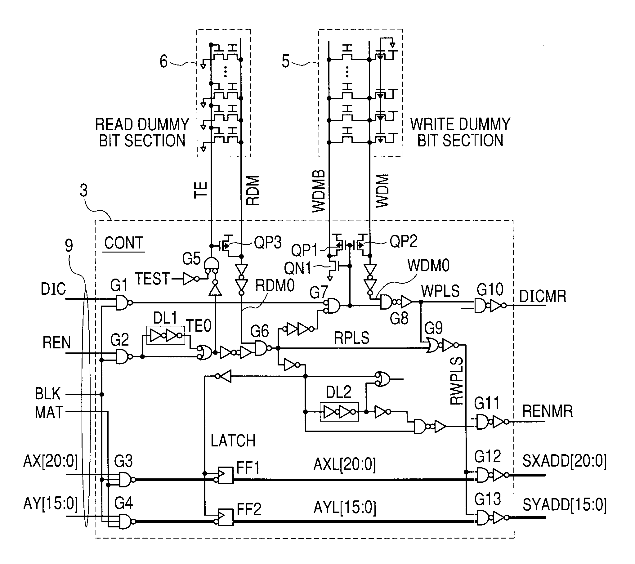
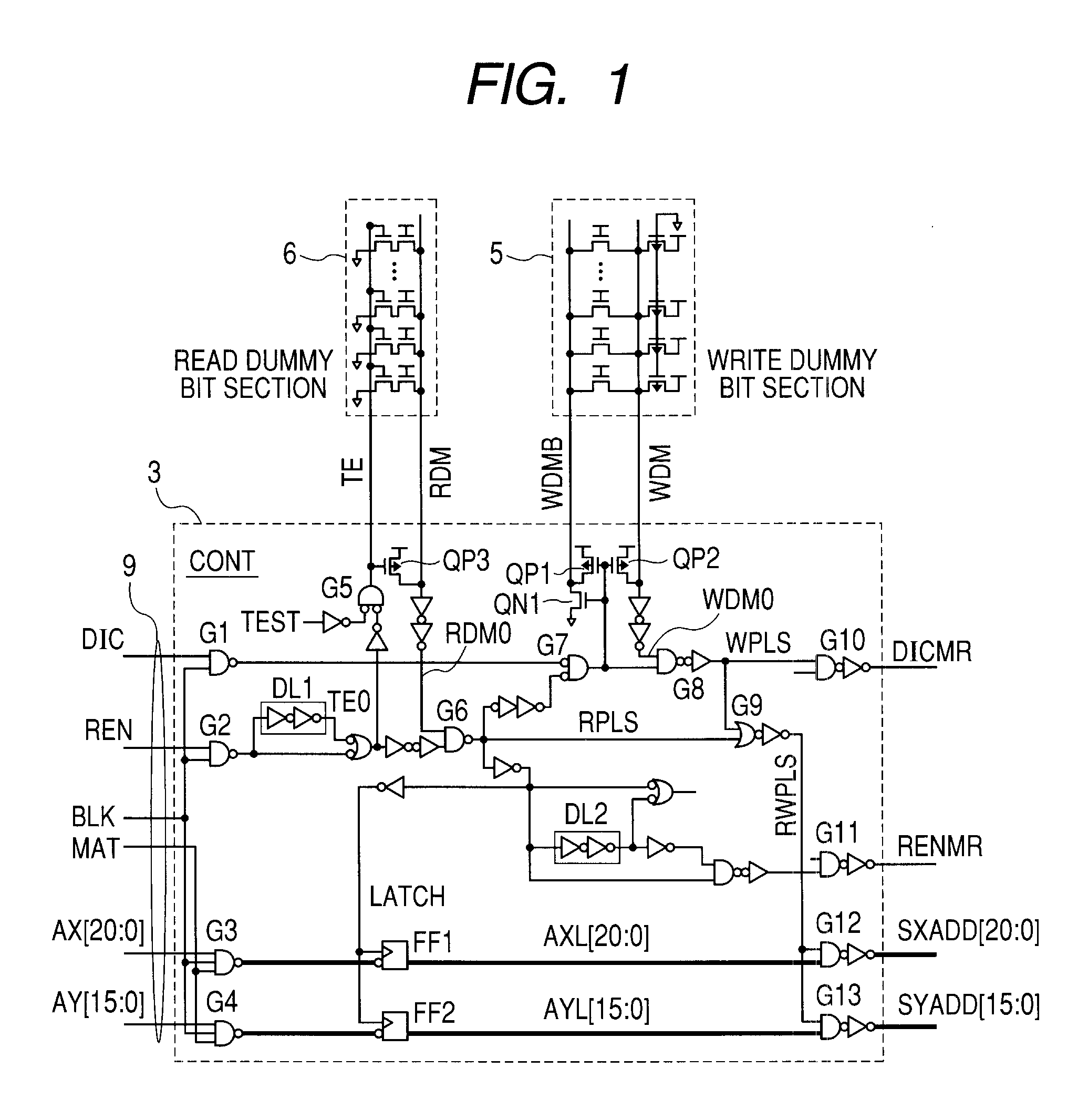
The patent text describes a semiconductor memory device that improves speed performance and adapts to variation in memory cell characteristics. The device includes a timing control circuit that selects dummy word lines and bit lines to adjust the timing of writing and reading to memory cells. The timing control circuit uses dummy cells that have the same ability to drive the actual memory cells. The device also includes a read dummy bit section and a write dummy bit section to simulate the characteristics of memory cells and improve consistency between the detection output signal and the operation of reading and writing the memory cells. The invention aims to enhance the speed performance of the memory device while minimizing the number of circuit elements.

Problems solved by technology

This SRAM arrangement has a problem in which, in particular, to make it adaptive to characteristic variation of memory cells, the SRAM requires even a greater number of dummy bit lines.
With smaller elements used, variation in characteristics of memory cells in one memory chip tends to become large.
Therefore, it is questionable that the implementation of timing adjustment with regard to the ability of driving the dummy cells 6 functions to compensate characteristic variation of the memory cells.
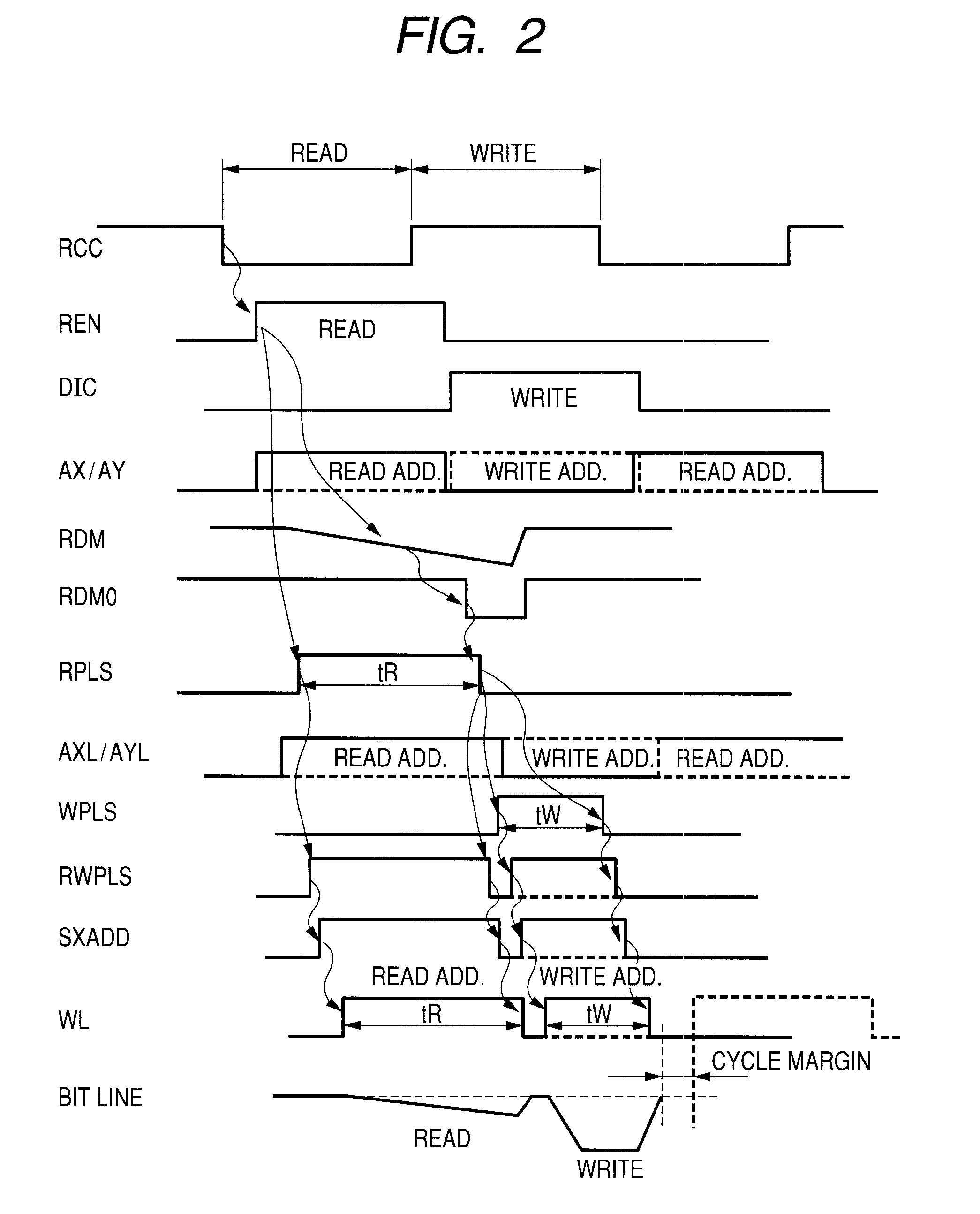
The timing adjustment in which a delay corresponding to the lowest ability of driving the dummy cells is selected is not effective for memory access in sync with an externally input clock cycle.
In consequence, delayed timing to terminate the current memory cycle by the timing adjustment as above overlaps the next memory cycle and an error occurs in the next memory cycle.

Method used


Image

  • Semiconductor memory device
  • Semiconductor memory device
  • Semiconductor memory device

Examples


Embodiment Construction

[0035]FIG. 3 shows a whole block diagram of an embodiment of an SRAM according to this invention. In FIG. 3, a layout of blocks is shown corresponding to their actual geometrical arrangement on a semiconductor chip. The semiconductor chip is divided into four areas, as indicated by dotted lines in the figure, the division being made by an address input circuit region extending lengthwise in the horizontal center and an indirect logic region extending crosswise in the vertical center. Although not restrictive, these four areas each have identical memory arrays and address / data logic regions. One area is divided into two arrays (9M arrays) in right and left positions. One array has a storage capacity of about 9 Mbits and, therefore, the whole chip has a storage capacity of 72 Mbits (9 Mbits×8).

[0036]FIG. 4 shows a detailed block diagram of one array from FIG. 3. One array (9M array) is divided into nine modules (1M modules) arranged in a lengthwise direction of FIG. 4 (also true for F...


PUM


Abstract

This invention provides a semiconductor memory device with enhanced speed performance or enabling timing adjustment reflected in characteristic variation of memory cells, adapted to suppress an increase in the number of circuit elements. A write dummy bit section comprises a first dummy line and a second dummy line corresponding to complementary bit lines and a plurality of first dummy cells formed to be similar in shape to static memory cells, wherein a write current path is coupled between the first dummy line and the second dummy line. In the write dummy bit section, one voltage level is input to the first dummy line through driver MOSFETs in relation to write signal inputs to the static memory cells and a signal change in the second dummy line precharged at the other voltage level is sensed and output. A timing control circuit deselects a word line selected by an output signal from the write dummy bit section.

Description

CROSS-REFERENCE TO RELATED APPLICATIONS [0001]The disclosure of Japanese Patent Application No. 2007-116379 filed on Apr. 26, 2007 including the specification, drawings and abstract is incorporated herein by reference in its entirety.BACKGROUND OF THE INVENTION[0002]This invention relates to a semiconductor memory device and relates to a technique that is effectively used for static RAMs in which high speed write and read operations are primarily performed.[0003]Japanese Patent Application Laid-Open No. 2006-004463 relates to a static RAM arranged to detect a write delay by using write dummy cells and / or detect a read delay by using read dummy cells and terminate a write operation and / or a read operation.[Patent Document 1][0004]Japanese Patent Application Laid-Open No. 2006-004463SUMMARY OF THE INVENTION[0005]In Patent Document 1, a transmission delay of a write enable signal is substituted by a delay involved in driving a dummy word line and a delay involved in writing to a memory...

Claims


Application Information

Patent Timeline
Patent Type & Authority Applications(United States)
IPC IPC(8): G11C5/06G11C7/00G11C11/00
CPCG11C7/22G11C7/227G11C11/412G11C11/419G11C2207/229
Inventor SHINOZAKI, MASAOSATO, HAJIME
Owner RENESAS ELECTRONICS CORP
Learn More