Semiconductor integrated circuit, semiconductor integrated circuit design support device, and semiconductor integrated circuit manufacturing method

a semiconductor integrated circuit and integrated circuit technology, applied in the field of semiconductor integrated circuit design support devices, semiconductor integrated circuit manufacturing methods, can solve the problems of increased chip area, increased power consumption, messed up setup timing, etc., and achieve high failure detection rate, reduced failure detection rate, scan

Active Publication Date: 2008-09-11
RICOH KK
View PDF15 Cites 2 Cited by
  • Summary
  • Abstract
  • Description
  • Claims
  • Application Information

AI Technical Summary

Benefits of technology

[0010]In conventional scanning techniques, failure detection rates may be reduced if their scan rates are lowered. In view of this, it is an object of the present invention to manufacture a semiconductor integrated circuit capable of maintaining a high failure detection rate even if the scan rate is lowered, while reducing the trend toward increased chip areas, increased power consumption, degraded timing convergence, and degraded wiring convergence of layouts by lowering the scan rate.
[0019]According to the embodiments of the present invention, it is possible to design a scan path without increasing the area of a semiconductor integrated circuit and messing up set-up timing. Furthermore, it is not necessary to take a measure for failure detection for a redundant circuit part as typically found in scanning relative to the configuration of shift registers, thereby simplifying a scan design.
[0020]Furthermore, it is possible to structure a scan path without making as many flip-flops as possible into scan cells, thereby designing the scan path while preventing an increase in entire area of a semiconductor integrated circuit. Moreover, it is possible to prevent an increase in chip area, increased power consumption, degraded timing convergence, and degraded wiring convergence of layouts, which are the problems caused by conventional scan designs.

Problems solved by technology

Then, the areas of the scan cells become large, resulting in set-up timing being messed up.
Recently, with scaling-up and high integration of semiconductor integrated circuits and an improvement in operating frequency, problems have emerged such as increased chip area, increased power consumption, degraded timing convergence, and degraded wiring convergence of layouts, which are caused by the scan designs.
However, taking such a measure will disadvantageously sacrifice a high failure detection rate.

Method used


Image

  • Semiconductor integrated circuit, semiconductor integrated circuit design support device, and semiconductor integrated circuit manufacturing method
  • Semiconductor integrated circuit, semiconductor integrated circuit design support device, and semiconductor integrated circuit manufacturing method
  • Semiconductor integrated circuit, semiconductor integrated circuit design support device, and semiconductor integrated circuit manufacturing method

Examples


first embodiment

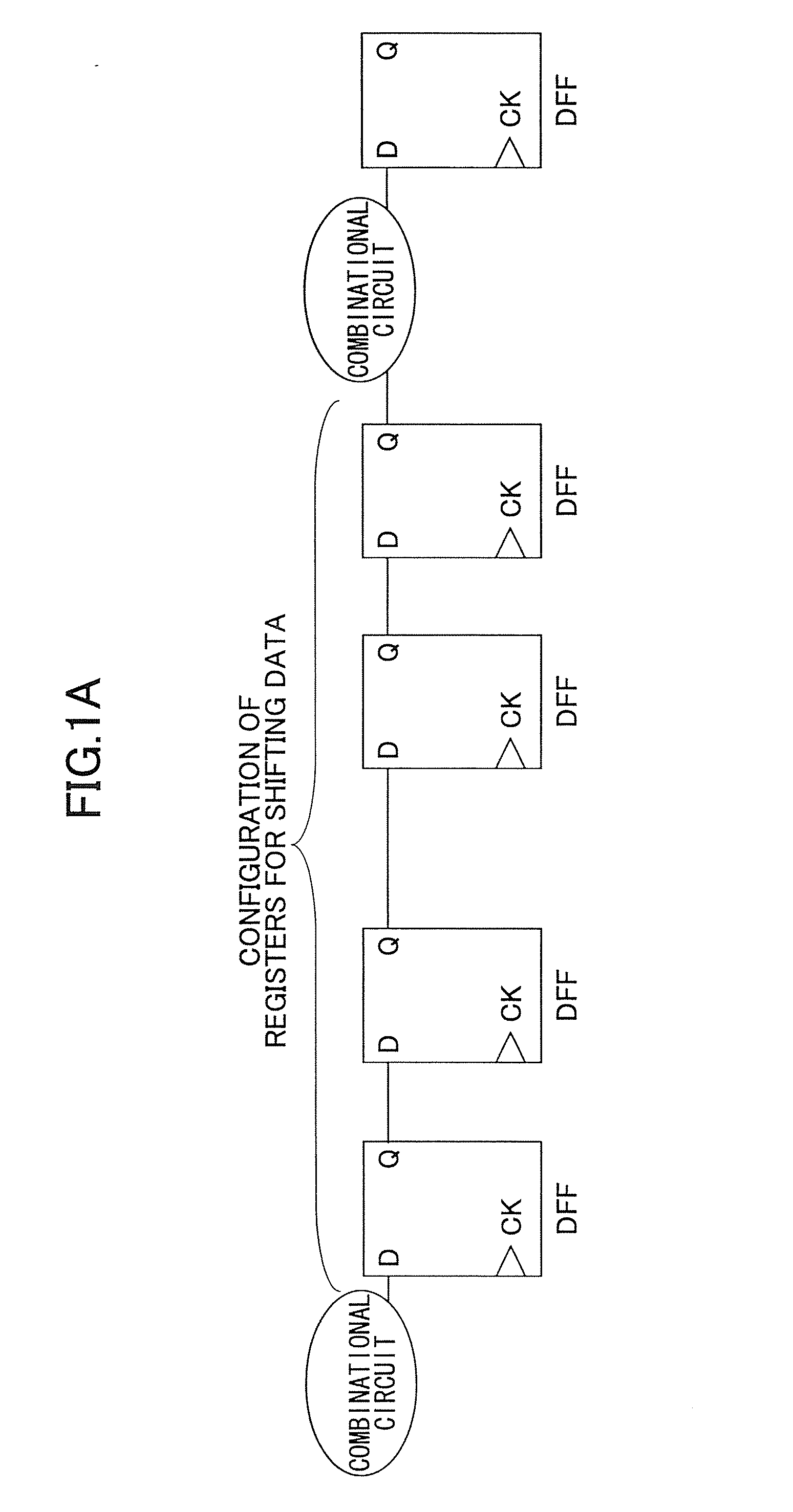
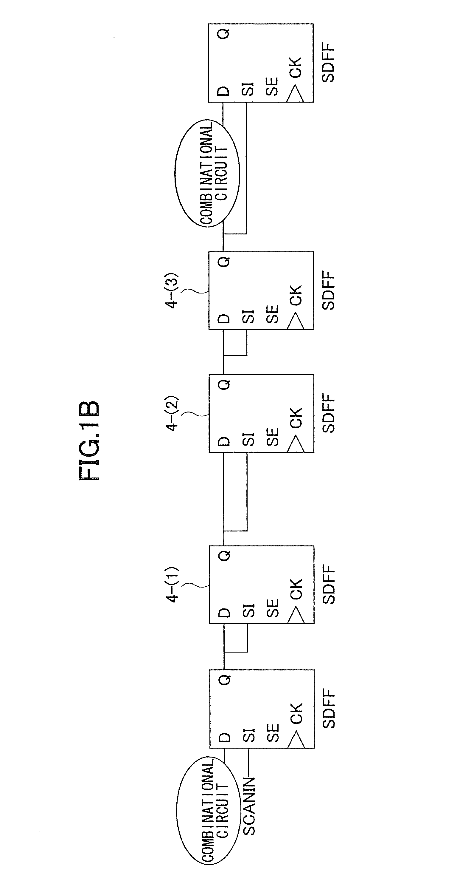
[0030]FIG. 1A shows an example of a general logic circuit particularly including a part configured of registers for shifting data, representing a schematic circuit diagram before scan insertion. As opposed to this, FIG. 1B shows the general logic circuit as shown in FIG. 1A including a scan path in which scan insertion is structured by conventional scan designs.

[0031]In the circuit as shown in FIG. 1B, a scan shift operation and a capture operation relative to both D input and SI input are the same in scan cells 4-(1), 4-(2), and 4-(3). In other words, the circuit as shown in FIG. 1B has a redundant circuit configuration.

[0032]FIG. 1C shows an example logic circuit diagram designed by a semiconductor integrated circuit designing method (manufacturing method) according to a first embodiment of the present invention. FIG. 1C is made by structuring a scan path in the logic circuit as shown in FIG. 1A, but it has flip-flops 6-(1), 6-(2), and 6-(3) as they are (see FIG. 1B). Note, howeve...

second embodiment

[0034]FIG. 2A shows an example of a general purpose parallel / serial conversion circuit. Here, if a “load_n” signal is “0,” data from combinational circuits are loaded in respective registers. If the “load_n” signal is “1,” the data loaded in the respective registers are shifted.

[0035]As opposed to this, FIG. 2B shows an example circuit diagram of a parallel / serial conversion circuit designed by a semiconductor integrated circuit designing method (manufacturing method) according to a second embodiment of the present invention. The circuit as shown in FIG. 2B is made by inserting a control circuit 8 in the circuit as shown in FIG. 2A. The control circuit 8 takes an OR of a “load_n” signal and a scan enable signal SCANEN. Then, if the SCANEN is “0,” the parallel / serial conversion circuit operates normally. If the SCANEN is “1,” the parallel / serial conversion circuit performs a data shift operation. Thus, the circuit as shown in FIG. 2B is capable of performing a scan operation and the ...

third embodiment

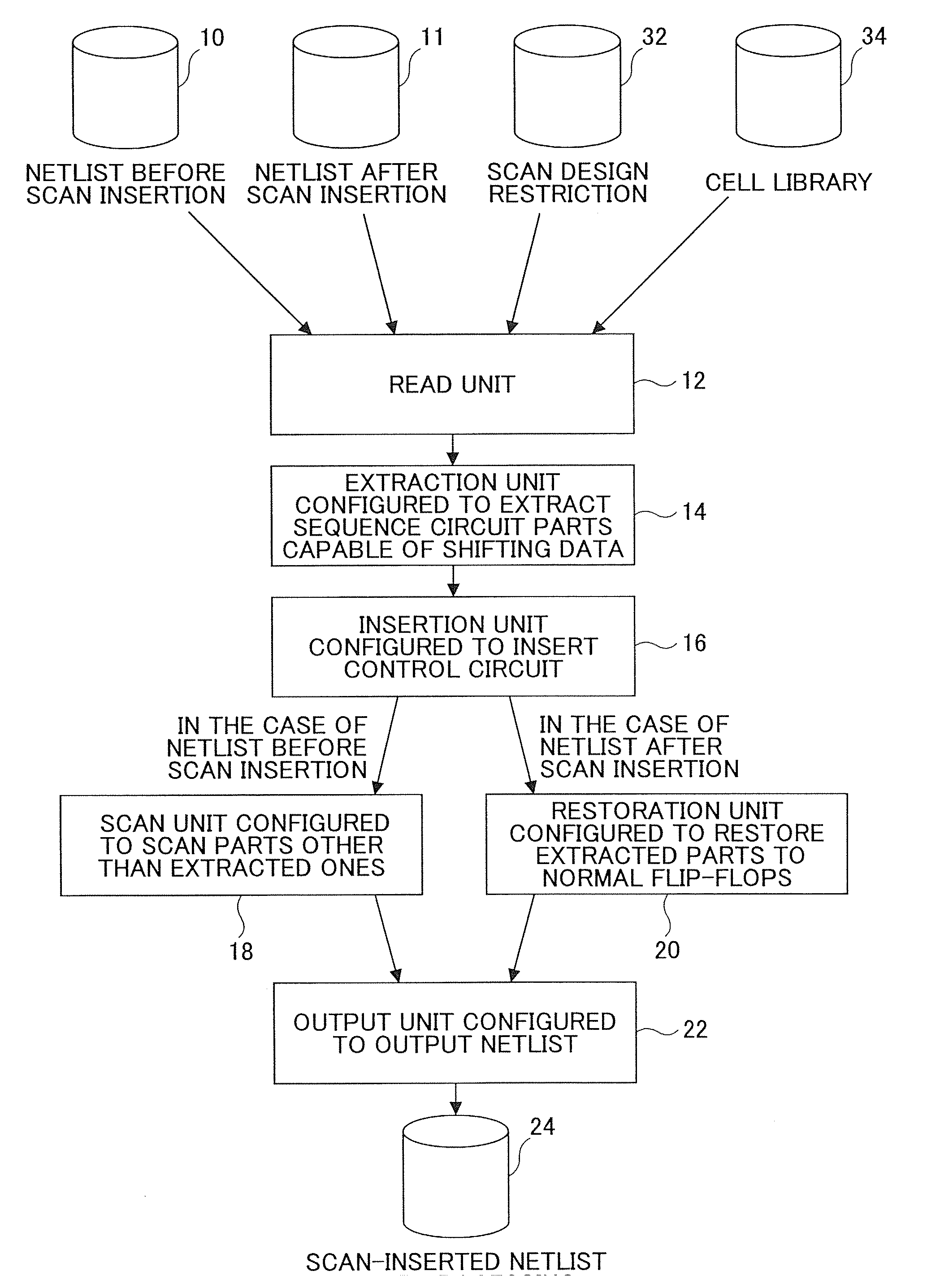
[0037]FIG. 3 shows a block diagram of a semiconductor integrated circuit design support device according to a third embodiment of the present invention. The respective units as described below constituting the semiconductor integrated circuit design support device according to the third embodiment are preferably realized by the installation of suitable programs in a suitable computer. Furthermore, data to be used or generated in the respective units constituting the device are preferably stored in various memories or storage media attached to the computer.

[0038](1) Netlist Processing Before Scan Insertion

[0039]At the beginning, a description is made of processing by the semiconductor integrated circuit design support device relative to a netlist 10 before scan insertion. First, a read unit 12 reads the netlist 10 before scan insertion.

[0040]Then, an extraction unit 14 for extracting sequence circuit parts capable of shifting data extracts circuit parts that can similarly perform the...


PUM

PropertyMeasurementUnit
areasaaaaaaaaaa
areaaaaaaaaaaa
structureaaaaaaaaaa

Abstract

A semiconductor integrated circuit including a user logic circuit is disclosed in which circuit parts for shifting data are composed of registers other than scan cells except for the circuit part right after a combinational circuit, and the parts configured of the registers other than the scan cells are used as a scan path.

Description

BACKGROUND OF THE INVENTION[0001]1. Field of the Invention[0002]The present invention relates generally to semiconductor integrated circuits, semiconductor integrated circuit design support devices, and semiconductor integrated circuit manufacturing methods and, in particular, to a semiconductor integrated circuit having a design for testability, a semiconductor integrated circuit design support device, and a semiconductor integrated circuit manufacturing method.[0003]2. Description of the Related Art[0004]Semiconductor integrated circuits are generally provided with scan cells for conducting a scan test. Taking, for example, in MUX (multiplex) scan cells, a multiplexer is inserted so that a data input of a normal flip-flop is switched to a scan input using a scan enable signal as one of the selectable signals. Then, the areas of the scan cells become large, resulting in set-up timing being messed up.[0005]As scan path designs, there are a full scan design and a partial scan design....

Claims


Application Information

Patent Timeline
Patent Type & Authority Applications(United States)
IPC IPC(8): G06F17/50H03K19/00H01S4/00
CPCG06F17/505Y10T29/49002G06F2217/14G06F30/327G06F30/333
Inventor SATOI, TOMOKINISHIGAKI, NAOHIKO
Owner RICOH KK
Why Eureka
Try Eureka