Eureka AIR delivers breakthrough ideas for toughest innovation challenges, trusted by R&D personnel around the world.

Method and arrangement for manufacturing optical products with complex three-dimensional forms

a manufacturing method and technology of optical products, applied in the field of optical microstructure manufacturing methods, can solve the problems of limiting the fabrication of preferred structures, reducing the production efficiency of optical microstructures, etc., to achieve the effect of eliminating design iterations, easy management and modification, and convenient adjustment of pattern density

Inactive Publication Date: 2008-08-21
MODILIS HLDG LLC
View PDF6 Cites 9 Cited by
  • Summary
  • Abstract
  • Description
  • Claims
  • Application Information

AI Technical Summary

Benefits of technology

[0034]The utility of embodiments of the present invention arises from a plurality of issues. Firstly, the advanced step embossing (ASE) patterning method of embodiments of the invention can provide optical modulation with versatile and variable multi-dimensional surface relief patterns even on large patterning areas. Also the density of patterns can be easily adjusted. Secondly, designed configurations are easy to manage and modify. Further, immediate adjustment can be enabled and completed by real time measurements, which eliminates design iterations; e.g. target uniformity of a light guide design can be fixed and later achieved by adding more micro-optic patterns onto the desired layer surface in stepwise manner. The patterned target substrate, such as a polymer layer / plastic sheet, can provide a fully functional micro-optic sample or the actual end product. In addition, this sample can be utilized for tool preparation by means of electroplating. Additional mastering processes typically are not needed. Same basic stamping tools can be applied to many optical designs and patterns.
[0035]Embodiments of the presented solution can enable manufacturing of very small optical elements (e.g. DO lenses) and can support optical integration in the manufacturing (e.g. integrated LED optics). The number of process steps is also reduced, which cuts down the duration of the overall process and enables cost-savings. The embossing functionality may be tailored to many existing step embossing, imprinting or e.g. chip bonding devices with few component amendments, additions and / or software changes. The ASE patterning method may provide new opportunities for fabricating e.g. diffractive optics. It may suit numerous applications of LED illumination, which require special DO patterns. Two further base solutions include micro-optic, e.g. refractive and / or DO, light guide elements and corresponding transmission elements, for example. These solutions may be applied for example, to consumer products such as mobile terminals, televisions, personal digital assistants, wrist computers, without forgetting automotive industry, advertizing and traffic or street lighting, for example. In a further embodiment the method or arrangement of the invention may be used to manufacture opto-electronic surface designs in addition to or instead of micro-optic structures.

Problems solved by technology

These methods have certain disadvantages, which critically limit the fabrication of preferred structures.
The most critical issues relate to fabrication of complex three-dimensional shapes (like blazed gratings), flexible orientations / modulation capability, as well as large surface patterning.
Lithographic methods do not perform well with blazed / slanted or hybrid profiles.
On the other hand, wafers are generally provided in very limited sizes (e.g. 6 or 8 inch sizes), which sets additional burden for manufacturing of large surfaces with microstructures.
Thus the total process speed is limited and optical measurement can't be done simultaneously.
Consequently, the vertical positioning cannot be controlled in a clever manner, and a longer process time is thus required for the depth control.
However, there are still critical limitations, such as flexibility of structural orientations / modulation, difficulties in fabricating larger structures, large machining tolerances, etc. relating to the feasibility of such solutions.
The generated spots generally provide rather limited optical performance.
Despite of various existing methods for manufacturing different microstructures on a carrier surface the aforesaid problems have remain at least partially unsolved in the context of high-precision micro-optic products.

Method used


Image

  • Method and arrangement for manufacturing optical products with complex three-dimensional forms
  • Method and arrangement for manufacturing optical products with complex three-dimensional forms
  • Method and arrangement for manufacturing optical products with complex three-dimensional forms

Examples


embodiment 520

[0087]In embodiment 520 shown at the top of FIG. 5d, the stamping tool 534 includes a micro-optic structure 540 attached to the stamping head / manipulator arm 530 by vacuum (note the two vertical lines representing vacuum channels for carrying out an air-suck function), for example. In the case of heat embossing, the heat is conducted to the stamping tool 534 from the heat source via heat conductive material 532, preferably as accurately as possible. Further, an insulation, and / or stopper, and / or alignment member 536 is coupled to the stamping head 530 and / or the stamping tool 534; in the visualized case there is a small distance between the head 534 and the member 536. In stopper and / or alignment action the member(s) 536 guides the embossing such that the structure 540 deforms the surface area of the substrate 538 only to a predetermined depth and prevents the structure 540 from proceeding deeper. As a heat insulator, the member 536 prevents heat conduction from the stamping tool 53...

embodiment 522

[0088]In embodiment 522, the member(s) 536 may be positioned on the substrate 538 as a surface mask, for example.

[0089]In embodiment 524, the whole head 530 is heated, whereby integrated or substrate-based insulator and optionally depth control sheet / layer, are typically used.

[0090]In embodiment 526, the stamping tool 534 includes structure 540 arranged as a sufficiently elongated protrusion from the tool's surface such that upon pressing the tool 534 towards the substrate 538, the desired depth is reached prior to contact between the rest of the tool 534 or head 530 with the substrate 538. The remaining space can be utilized for air cooling, which can be enhanced by utilizing additional air blowing function as depicted by the curved arrow in the figure. In another, either alternative or supplementary embodiment the whole area under embossing and / or adjacent thereof may be air-cooled after the stamping tool 534 has been lifted up from the surface of the substrate 538.

[0091]In embodi...

embodiment 822

[0098]Embodiment 822 illustrates a number of different options for providing a micro-optic lens for the LED. In one embodiment 824, the lens includes a surface relief structure on the surface facing away from the LED. In another embodiment, the surface relief structure of the lens is provided on the surface facing towards the LED instead. Also, an additional layer (thin rectangle in the figure) between the lens including the relief structure and the LED casing can be provided. In a further embodiment 828, includes surface relief forms on both sides of the lens, i.e. it is a question of a double-sided lens, and again, an additional layer is included. The surface relief forms may have different micro-optic forms and the blazed and binary gratings were shown for illustrative purposes, as being appreciated by those skilled in the art.

[0099]Embodiment 830 includes an, in many cases advantageous, lens form, a so-called Fresnel-lens, is shown to highlight the varying and rather complex nat...


PUM

PropertyMeasurementUnit
Temperatureaaaaaaaaaa
Pressureaaaaaaaaaa
Structureaaaaaaaaaa

Abstract

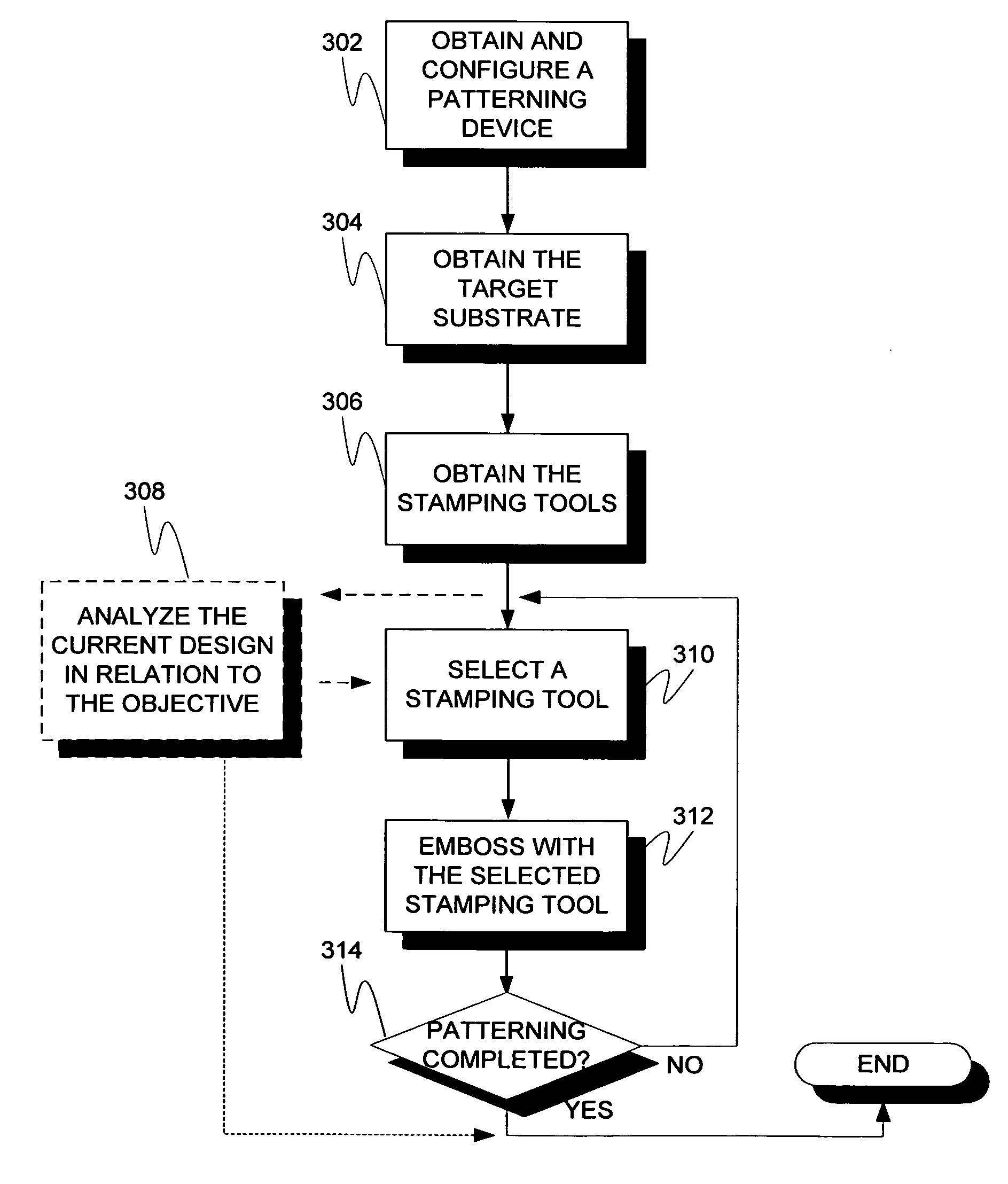
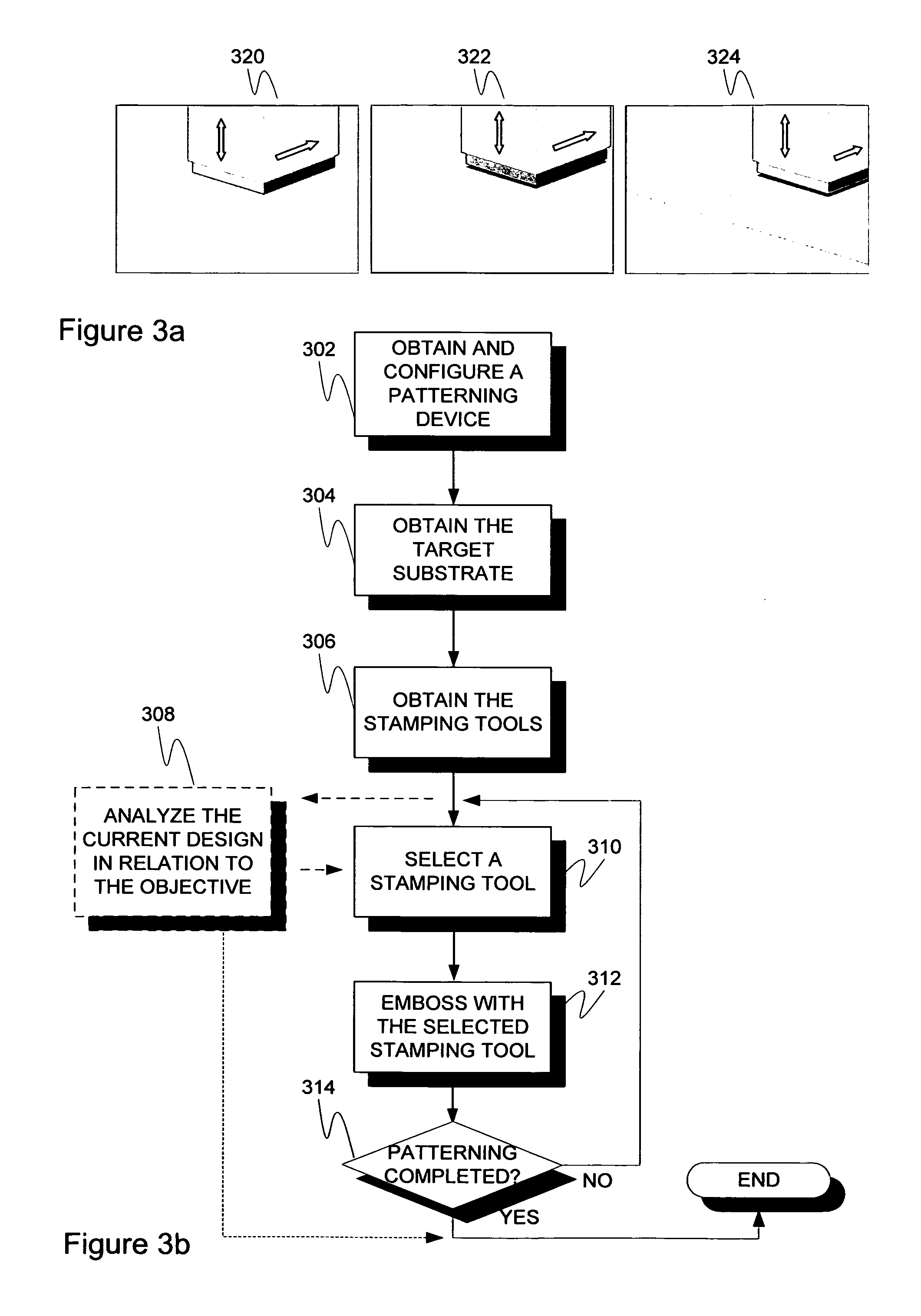
A method, an arrangement and computer program product for manufacturing micro-optic surface design with complex, variable three-dimensional forms. A step embossing, step imprinting, a chip bonding or a corresponding device capable of patterning the surface of a target substrate is obtained. The target substrate whereto the micro-optic structures shall be patterned is obtained. A plurality of different stamping tools operable with the device is obtained. Each stamping tool includes one or more surface relief forms defining one or more micro-optic structures. A stamping tool is selected from the plurality of stamping tools by the device. The target substrate is embossed with the selected stamping tool as controlled by the device. The selected stamping tool is optionally heated or assisted by at least one ultraviolet light so as to cure the target substrate during or after the embossing. The selecting and embossing steps are repeated until the micro-optic surface design has been completed on the substrate.

Description

CROSS-REFERENCE TO RELATED APPLICATIONS[0001]This application claims priority to U.S. provisional patent application 60 / 855,372, filed 31 Oct. 2006, the entire contents of the disclosure of which is hereby incorporated by reference.FIELD OF THE INVENTION[0002]Generally the invention relates to optics and opto-electronics. In particular the invention concerns manufacturing methods of optical microstructures.BACKGROUND OF THE INVENTION[0003]There is an ever-increasing demand for improving light management and luminous efficiency in many illumination applications. This hypothesis is especially applicable to LED (Light-Emitting Diode) illumination. It is necessary to utilize efficient optics with point-like light sources such as LEDs in order to achieve the required lighting performance. Solutions exploiting diffractive optics or other sophisticated micro-optic structures provide a range of new possibilities for advanced illumination including dimensional benefits and cost-effective int...

Claims


Application Information

Patent Timeline
IPC IPC(8): B44C1/24
CPCB29C59/02B29C59/00H01L21/68B29C67/00
Inventor RINKO, KARI
Owner MODILIS HLDG LLC
Why Eureka
Eureka Blog
Learn More