
Semiconductor storage device and manufacturing method thereof

Active Publication Date: 2008-08-07
RENESAS ELECTRONICS CORP
View PDF9 Cites 69 Cited by
  • Summary
  • Abstract
  • Description
  • Claims
  • Application Information

AI Technical Summary

Benefits of technology

[0033]As seen from Patent Document 4, it is found that a hole injection from a gate electrode is effective when degradation of a channel interface should be suppressed in a non-local hole injection system.
[0036]An object of the present invention is to provide a non-volatile semiconductor storage device which can perform a non-local hole injection from a gate electrode at a high efficiency while maintaining a thickness and a band offset of an insulating film under the gate electrode to secure a sufficient charge retention characteristic.
[0043]A non-volatile semiconductor storage device which can perform a non-local hole injection from a gate electrode at a high efficiency while maintaining a thickness and a band offset of an insulating film under the gate electrode to secure a sufficient charge retention characteristic can be realized.

Problems solved by technology

Especially, when a film thickness of an insulating film between the gate electrode and the charge accumulation layer is thick or when a barrier of the insulating film to the holes is high, an amount of electrons injected from the substrate is more than an injection amount of holes, which results in difficulty of injection of holes.
Naturally, a hole injection which does not use hot carriers is inferior to that using hot carriers in injection efficiency, so that a rewriting speed of the former becomes slower than that of the latter.
However, lowering of the band offset of the insulating film and thinning the insulating film between the gate electrode and the charge accumulation layer deteriorate retention characteristics of electrons and holes trapped in the silicon nitride film.

Method used


Image

  • Semiconductor storage device and manufacturing method thereof
  • Semiconductor storage device and manufacturing method thereof
  • Semiconductor storage device and manufacturing method thereof

Examples


first embodiment

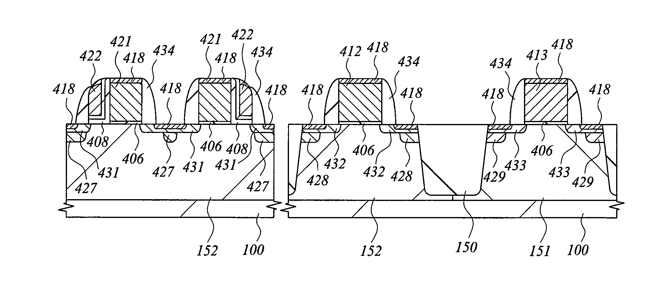
[0146]A high efficiency hole injection from a gate electrode side which is a feature of the present invention can be understood from an one-dimensional band structure in a direction perpendicular to a substrate. Then, a memory cell having the same device structure as that of an ordinary MOS transistor will be explained as a representative example. Thereafter, an electron injection method is examined and a case that the electron injection method is applied to a memory cell structure suitable for high-speed operation is explained. For the memory cell structures, an optimal structure according to applications of a memory can be selected.

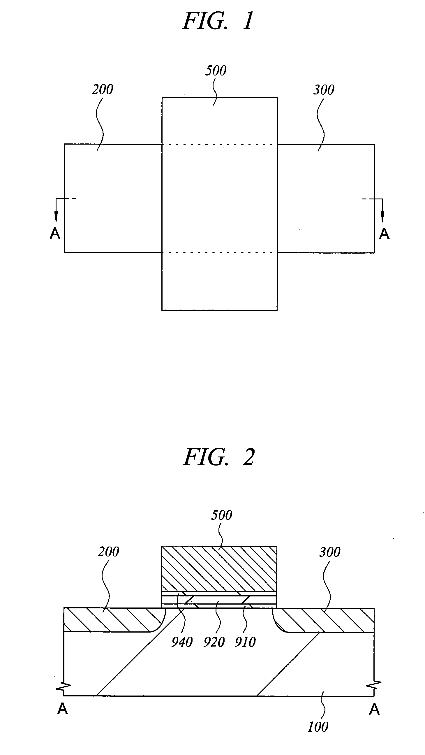
[0147]Manufacturing steps of a memory cell of the present embodiment will be explained with reference to FIG. 13 to FIG. 15, and FIG. 17. The figures correspond to a section A-A of a plan layout shown in FIG. 1, where explanations are made using a process technique corresponding to the so-called 0.13 μm generation.

[0148]As shown in FIG. 13, a device iso...

second embodiment

[0182]It is apparent from the above-mentioned first embodiment that a high efficiency hole injection from the gate electrode can be realized by lowering the potential barrier of the insulating film under the gate viewed from holes in polysilicon gate. In the present embodiment, lowering of the potential barrier with respect to holes in the gate is realized by using semiconductor materials with a wide gap for the gate electrode instead of by forming the quantum levels.

[0183]FIG. 29 shows a band diagram near a gate electrode when the gate electrode of a memory cell comprises a silicon carbide (SiC) film and a predetermined gate electrode voltage is applied thereto. A solid line CB (SiC) shown in a gate electrode part in figure denotes a conduction band of SiC, and a solid line VB (SiC) denotes a valence band of SiC, respectively. A dotted line CB (Si) denotes a conduction band of silicon and a dotted line VB (Si) denotes a valence band of silicon, respectively.

[0184]As described in IE...

third embodiment

[0186]The high efficiency hole injection from the gate electrode can also be realized by producing hot holes on the gate electrode. It can be said that this method lowers a barrier of the insulating film to holes in the gate electrode like the first and second embodiments.

[0187]In the present embodiment, as shown in a band diagram in FIG. 30, the gate electrode comprises a two-layered film made of an n-type polysilicon film and n+ type (or p+-type) polysilicon film with a high impurity concentration to generate avalanche hot holes. FIG. 30 is a band diagram near the gate electrode just after applying a gate voltage. Also, FIG. 30 shows production of the avalanche hot holes (Ha).

[0188]In order to produce the avalanche hot holes, it is necessary to accelerate carriers by deep depletion such as shown in FIG. 30, so that it is necessary to make an impurity concentration in the n-type polysilicon film near the gate electrode lower than 1018 atom / cm3. When the impurity concentration in th...


PUM


Abstract

In a non-volatile memory in which writing / erasing is performed by changing a total charge amount by injecting electrons and holes into a silicon nitride film serving as a charge accumulation layer, in order to realize a high efficiency of a hole injection from a gate electrode, the gate electrode of a memory cell comprises a laminated structure made of a plurality of polysilicon films with different impurity concentrations, for example, a two-layered structure comprising a p-type polysilicon film with a low impurity concentration and a p+-type polysilicon film with a high impurity concentration deposited thereon.

Description

CROSS-REFERENCE TO RELATED APPLICATION[0001]The present application claims priority from Japanese Patent Applications No. JP 2007-023301 filed on Feb. 1, 2007, and No. JP 2007-155472 filed on Jun. 12, 2007, the contents of which are hereby incorporated by reference into this application.TECHNICAL FIELD OF THE INVENTION[0002]The present invention relates to a semiconductor storage device and a manufacturing method thereof and, in particular, to an effective technique applied to a semiconductor storage device including a non-volatile memory using hole injection from a gate electrode and hot electron injection from a semiconductor substrate as a carrier injection system.BACKGROUND OF THE INVENTION[0003]Currently, LSIs obtained by integrating semiconductor devices are used for controlling various systems to constitute infrastructures supporting society. Since an operation of a current LSI is based upon conduction of an arithmetic processing according to a program, in most cases, it is i...

Claims


Application Information

Patent Timeline
IPC IPC(8): H01L27/088
CPCG11C16/0466H01L21/28273H01L21/28282H01L27/105H01L27/115H01L29/792H01L27/11526H01L27/11568H01L27/11573H01L29/42344H01L29/513H01L27/11521H01L29/40114H01L29/40117H10B41/40H10B43/40H10B43/30H10B69/00H10B41/30
Inventor YANAGI, ITARUMINE, TOSHIYUKIHAMAMURA, HIROTAKAHISAMOTO, DIGHSHIMAMOTO, YASUHIRO
Owner RENESAS ELECTRONICS CORP
Learn More