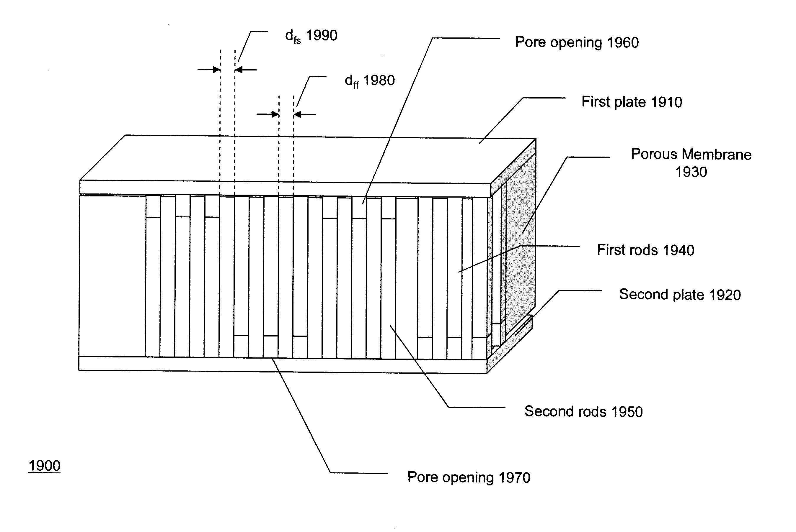
NANO scale digitated capacitor
a capacitor and nano-scale technology, applied in the field of nano-scale capacitors, can solve the problems of capacitance size, typically difficult if not impossible to achieve, and achieve the effect of increasing the capacitan
- Summary
- Abstract
- Description
- Claims
- Application Information
AI Technical Summary
Problems solved by technology
Method used
Image

Examples
experiment 1
pacitor
[0097]Both a PC membrane and PET membrane were tested in this example. There was no silver print electrode on one side of the membrane surface. Copper tape held by a weight was used as the electrode (the other side was PVD).
[0098]Supplies and Equipment:
[0099]1. PC and PET membranes pre-filled with gold.
[0100]2. Capacitance measuring device—DVM 638 Multitester.
[0101]3. Copper tape ¼ inch width (electrodes).
[0102]4. PVD layer of the membrane served as one electrode.
[0103]Results:
[0104]The measured results demonstrate a higher capacitance for the digitated PC and PET membranes, as shown in Table 6. The closed-formed solution of a parallel plate PC capacitor should be approximately 214 pF (for a square centimeter with a dielectric constant of 2.9). The measured value was 21.4 pF, off an order of magnitude. For the PET capacitor, the value should be 221 pF, and the measured value was 11.3 pF. The lower value is likely due to the copper tape not lying completely flat on the membran...
experiment 2
pacitor with Longer Metal Rods and Larger Capacitance.
[0106]Supplies and Equipment:
[0107]1. PC membranes, 200 nm diameter pores.
[0108]2. Silver print used as electrode.
[0109]3. Potentiostat used to deposit copper into pores applying −500 mV.
[0110]4. Capacitance measuring device—Scope DVM 638 Multitester and Potentiostat Model 273 FG&G Princeton Applied Research.
[0111]5. Copper tape ¼ inch width.
The silver layer of the membrane served as one electrode while copper tape covered the other side.
[0112]Results:
[0113]Table 7 gives the results for the parallel plate capacitors measured for five different devices, with the average capacitance being 92 pF (standard deviation of +1-19. pF). These results are with no metal in the pores. Again, the values are smaller then the results for the digitated capacitor (Table 1.3), verifying that the digitated capacitor results in a larger capacitance.
TABLE 7PC parallel-plate capacitorsParallel-plate Cap #Capacitance(Date: Mar. 11, 2005)(pF / cm2)#194#275...
experiment 3
pacitor: Time-to-Charge Analysis
[0134]A commercial polycarbonate (PC) membrane-template structure was used to build a digitated capacitor. The membrane had 200 nm diameter pores, and a thickness on the order of 12 μm. Copper was the metal used to fill the pores, applying the standard electrodeposition process discussed above.
[0135]FIG. 10A shows the current response versus time to charge of the digitated capacitor with 10 mV DC of applied voltage over a period of 30 seconds with a 9.95 KΩ series resistor. Note the characteristic curve of the capacitor of the present invention as compared to the commercial capacitor of FIG. 9A. While similar to the commercial capacitor, there appears an almost linear decrease over time after an initial exponential decrease. A discussion of the novel discharge characteristics will be discussed later with regard to FIG. 14 where a commercial capacitor discharge is plotted along with that of the present invention. If the exponential portion of this curv...
PUM
| Property | Measurement | Unit |
|---|---|---|
| Length | aaaaa | aaaaa |
| Length | aaaaa | aaaaa |
| Pore size | aaaaa | aaaaa |
Abstract
Description
Claims
Application Information
 - R&D
- Intellectual Property
- Life Sciences
- Materials
- Tech Scout
- Unparalleled Data Quality
- Higher Quality Content
- 60% Fewer Hallucinations
Browse by: Latest US Patents, China's latest patents, Technical Efficacy Thesaurus, Application Domain, Technology Topic, Popular Technical Reports.
© 2025 PatSnap. All rights reserved.Legal|Privacy policy|Modern Slavery Act Transparency Statement|Sitemap|About US| Contact US: help@patsnap.com